Basic Electronics (MCQs With Explanatory Answers)
Basic Electronics (MCQs With Explanatory Answers)
 Q1. Choose the below option in terms of ascending order of band gap energy
Options
- Diamond, Graphite, Silicon
- Graphite, Silicon, Diamond
- Silicon, Graphite, Diamond
- Silicon, Diamond, Graphite
Explanatory Answer: Diamond has the highest bandgap energy, about 6eV. It is this high bandgap which separates the filled valance band from the conduction band and makes Diamond an insulator. Though Graphite is also a form of Carbon, like Diamond, its crystal symmetry is different and band gap energy is about 1eV, making it a conductor. Bandgap energy of Silicon is about 1.21eV, which can be acquired only with increase in temperature, making it a semiconductor.
Show Explanatory Answer
Q2. Band gap Energy for Silicon and Germanium at Room Temperature (300°K) are ____ & ____ respectively: –
- 56eV, 1.1eV
- 72eV, 1.2eV
- 1eV, 0.72eV
- 1eV, 0.56eV
Explanatory Answer Below are the band gap energy relations with temperature for both Silicon and Germanium Egsi (T) = 1.21 – 3.60 x 10⁻⁴ Egge (T) = 0.785 – 2.23 x 10⁻⁴ Substituting T = 300 in both the above equations, we get Bandgap energies as given below; Egsi (300) = 1.1 eV Egge (300) = 0.72 eV
Show Explanatory Answer
Q3. Electrical characteristics of a semiconductor depends on concentration of free electrons and holes.
- True
- False
Explanation: Current Density in any conducting material is given as: J=( nµn + pµp ) eE= σE Where, n = concentration of electrons, p = concentration of holes, e = charge, E = applied electric field, and σ = conductivity. Thus it can be seen that the electrical characteristics depends on concentration of electrons and holes. Thus, the above statement is true.
Show Explanatory Answer
Q4. Transport of charge carriers in semiconductor is achieved through: –
- Conduction and Diffusion
- Conduction
- Diffusion
- None of the above
Explanatory Answer: Two ways in which charge carriers are transferred in semiconductor are – conduction and diffusion Conduction in semiconductor is accomplished by movement of free electrons and holes. While electrons are negative charge carrying particles, holes are positive charge carrying particles. Both their current is in same direction. Diffusion is caused by movement of charge carriers from higher concentration area to lower concentration area. This is possible because of non-uniform concentration in semiconductors.
Show Explanatory Answer
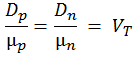
Q5. The electron mobility of Germanium at room temperature (in Kelvins), for an electron diffusion constant of 99 is approximately: –
- 3200 cm2/V-sec
- 4500 cm2/V-sec
- 3800 cm2/V-sec
- 2000 cm2/V-sec
Explanatory Answer: As per Einstein’s equation for diffusion, Where, Dn = Electron Diffusion Constant, DP = Hole Diffusion Constant, µp = Hole Mobility, µn = Electron Mobility and VT = Volt equivalent of temperature, = T/11600. At room temperature, i.e. T = 300°K, VT = 0.0258 V approx Substituting Dn = 99 and VT = 0.025 in the above equation, we get µn = 3837.20 or 3800 approx.
Show Explanatory Answer
Q6. Carrier lifetime for holes and electrons in a semiconductor ranges from –
- Milliseconds to hundreds of nanoseconds
- Microseconds to seconds
- Nanoseconds to hundreds of microseconds
- Nanoseconds to thousands of milliseconds
Explanation: For an intrinsic semiconductor with equal concentration of holes and currents, the carrier lifetime for free electrons and holes is determined by the rate of recombination. While new electron-hole pairs are formed due to thermal agitation, existing electron-hole pair disappear due to recombination.
Show Explanatory Answer
Q7. Which metal among these is widely used as a recombination agent by semiconductor manufacturers to obtain desired carrier lifetime of charge carriers?
- Silver
- Gold
- Iron
- Aluminum
Explanation: Addition of metallic impurities in the semiconductor introduces new energy states in the forbidden gap of the semiconductor crystal, thus increasing the level of recombination.
Show Explanatory Answer
Q8. The Hall effect is used to determine the
- Only the carrier concentration of semiconductors
- Current flowing across a semiconductor
- Type of semiconductor and carrier concentration
- None of the above
Hall effect is the phenomenon of induction of electric field in a semiconductor specimen carrying current of magnitude I, when placed in a transverse magnetic field, B. If current is in positive X direction, Magnetic field is in positive Z direction, force will be exerted in negative Y direction. The polarity of voltage, VH across the specimen determines whether it is N-type or P-type. Also, carrier concentration is determined as: n (p) = ρ/e, where ρ = charge density and e is magnitude of charge Now, ρ = 1/RH,, where RH is Hall coefficient and is given as: RH = VHw/BI w = width of the specimen in direction of magnetic field.
Show Explanatory Answer
Q9: The thickness of space charge region for a P-N junction diode is of the order of :-
- 10-4 cm
- 10-2 cm
- 10 cm
- 100 cm
Explanatory Answer: For a P-N junction diode, the space charge region is the region devoid of mobile charge carriers near to the junction. The electro-static potential variation in this region forms a potential barrier which opposes further diffusion of opposite charge carriers across the junction.
Show Explanatory Answer
Q10. Formation of a junction between a sample of P-type and N-type material causes _______ action
- Rectifying
- Conducting
- Insulating
- None of the above
Explanatory Answer: Addition of donor atoms into one side of an intrinsic semiconductor (like Germanium) and acceptor atoms into another side, causes formation of a junction. Under no external applied electric field, a potential barrier exists across the junction due to formation of depletion region (depletion of mobile charge carriers). However, when an external electric field is applied such that p-region is of positive polarity and n-region is of negative polarity, the potential barrier is reduced, causing flow of current. This is called Forward biasing. When the opposite occurs, i.e. p-region is of negative polarity and n-region is of positive polarity, the potential barrier is increased, hindering the flow of current. Thus, since the p-n junction device would allow flow of electricity in only one half of the electric signal, but not in the other half, this constitutes rectifying action.
Show Explanatory Answer
Q 11. Cut-In or breakdown voltage of Silicon diode is greater than that of Germanium diode because ______.
- Reverse saturation current in a Silicon diode is lesser than that in Germanium diode
- Reverse saturation current in Germanium diode is lesser than that in Silicon diode
- The current is initially less dependent on voltage for a Silicon diode
- None of the above
Explanatory answer: For a Germanium diode, the breakdown voltage is about 0.2 V, whereas that of Silicon diode is 0.6 Volts. The reason being that, reverse saturation current in a Ge diode is about 1000 times more than that in Si diode. Also, current flowing through the diode is as given below; I = Io ( e V/ηVT – 1 ) For Ge, the symbol η = 1, whereas that for Si is 2 for small currents and 1 for large currents. Hence, for first several tenths of volts, the current varies as e V/2VT.
Show Explanatory Answer
Q 12. For intrinsic Germanium, the change in conductivity per degree rise in temperature is: –
- Increases approximately by 6%
- Decrease approximately by 8%
- Increases approximately by 5%
- Remains unchanged
Explanatory answer: Intrinsic concentration for any semiconductor is as given below; ni2 = Ao T3 e -EGO / kT) Conductivity of intrinsic Germanium varies with concentration as given below; σ = ni (µn+ µp ) e Substituting the constant values for intrinsic Germanium and merging both the above equations, we get that conductivity increases by approximately 6% per degree rise in temperature.
Show Explanatory Answer
Read More Here : Electrical & Electronics Engineering MCQS with Explanatory Answers


Good Day!!
Many thanks for creating such a nice & helpful WEBSITE. BRAVO. Keep it up.
If someone has really – thoroughly studied the relevant subject, then he / she would be able to answer the questions.
I left my studies many many years back, so few of my answers were Wrong. I have to keep myself up-to-date.
Thanks Again – Keep Coming
Very Best Regards
Abdur Rab
Good Question & Answer , That very helpful for Beginner.
Good effort
You had really put in a lot effort in developing the materials.
Awesome, Keep it up!!!
Thank you.