Exclusive-NOR (XNOR) Digital Logic Gate
Exclusive-NOR Gate - Digital Logic XNOR Gate
Exclusive-NOR Gate – Digital Logic XNOR Gate
What is Logic XNOR or Exclusive-NOR Gate?
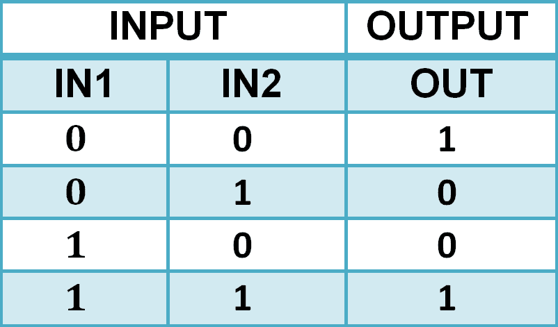
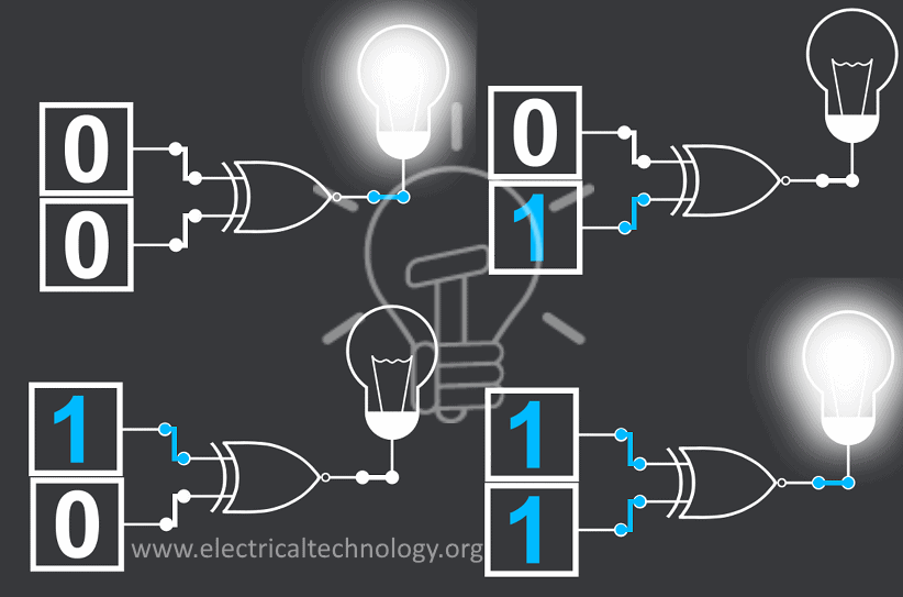
XNOR gate also known as Exclusive-NOR or Exclusive-Negative OR gate is “A logic gate which produces High state “1” only when there is an even number of High state “1” inputs”.
For 2-input gate, it can be interpreted as when both of the inputs are same, then the output is High state and when the inputs are different, then the output is Low state “0”.
XNOR gate can have two or more than two inputs but it has only one output. This gate is also used for equality.
XNOR Gate Logic Symbol, Boolean Expression & Truth Table
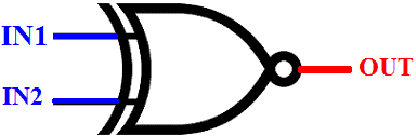
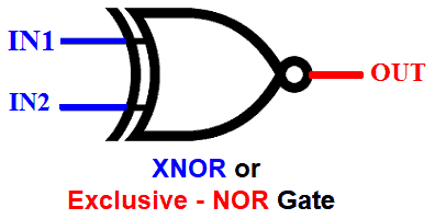
XNOR Gate Symbol
There are 3 types of symbols used for XNOR gate all over the world.
American National Standards Institute (ANSI)/ MILITARY
International Electrotechnical Commission (IEC)/EUROPEAN 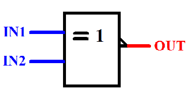
Deutsches Institut für Normung (DIN)/GERMANY XNOR gate
Boolean Expression
OUT = ( I̅N̅1̅ & I̅N̅2̅) + (IN1 & IN2) or OUT = (I̅N̅1̅ + IN2) & (IN1 + I̅N̅2̅)
OR
![]()
Truth Table
XNOR Gate Logic flow Schematic Diagram
Construction and Working Mechanism of XNOR Gate
XNOR Gate Using BJT and Diodes
Schematic of XNOR gate using Diodes and BJT (NPN transistor) is given below. In which we have used one NPN transistor, 4 diodes and the resistor between Diode Bridge and NPN is used in series configuration because BJTs operates on input current, not input voltages.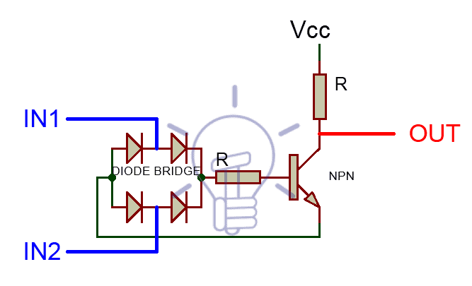
The diodes are used in a bridge configuration (Rectifier) to sort out the input logic into the positive level, means if there is a High state input it will always flow to the base of NPN to switch it on. And the Low state will always flow out to the emitter of NPN transistor.
The transistor is used for switching upon the input logic given to it.
When inputs are different, the high state flow to NPN transistor’s base and turn it ON. The LOW state “0” flow through the negative side of the bridge and flow through NPN’s emitter as output.
When the inputs are same, if it’s LOW state “0” then NPN will never turn on because there be no HIGH state input at its base. So Vcc will flow out as logic high state “1” output. If it’s HIGH state “1” then the NPN will turn on but there will be no Logic 0 to flow through the emitter. So again Vcc will flow out as HIGH state”1” output.
XNOR Gate Using MOSFET and Diodes
Discrete XNOR gate can be made with MOSFET and diodes. XNOR schematic using NMOSFET and diodes is given below. 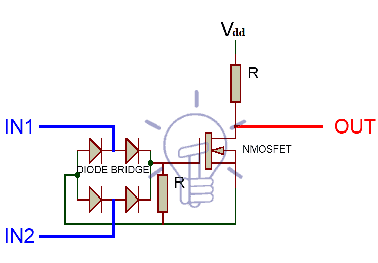
In this schematic 4 diodes are used in a bridge configuration for sorting out input logic. NMOSFET is used for switching upon input logic. The resistor between Diode Bridge and MOSFET is used in parallel configuration because MOSFETs operates on Gate’s voltages, not current.
When both inputs are different, then the High state will flow to NMOSFET’s gate and the LOW state will flow to NMOSFET’s source to build up potential at its gate, which will switch it ON. And the LOW state “0” will flow out as output.
When both of the inputs are same i.e. if both are HIGH state “1” than the HIGH state will flow to the gate of NMOSFET but there will be no potential at its source so NMOSFET will switch OFF. Hence Vdd (HIGH state “1”) will flow out as HIGH state “1” output. When both inputs are LOW state “0”, again there will be no potential (voltage) at the gate of NMOSFET so it will never turn ON and Vdd will flow out as HIGH state “1” output.
XNOR Gate From other Logic Gates: (Combinational Logic)
XNOR operation can be achieved with a combination of different logic gates.
Boolean expression of XNOR is given below.
Sum of Product
In this expression, we use the sum of Min terms. Min terms are the product of inputs for which output is HIGH state “1”.
SOP expression can be easily implemented with NAND gates.
According to the truth table given above the SOP (sum of product) expression is:
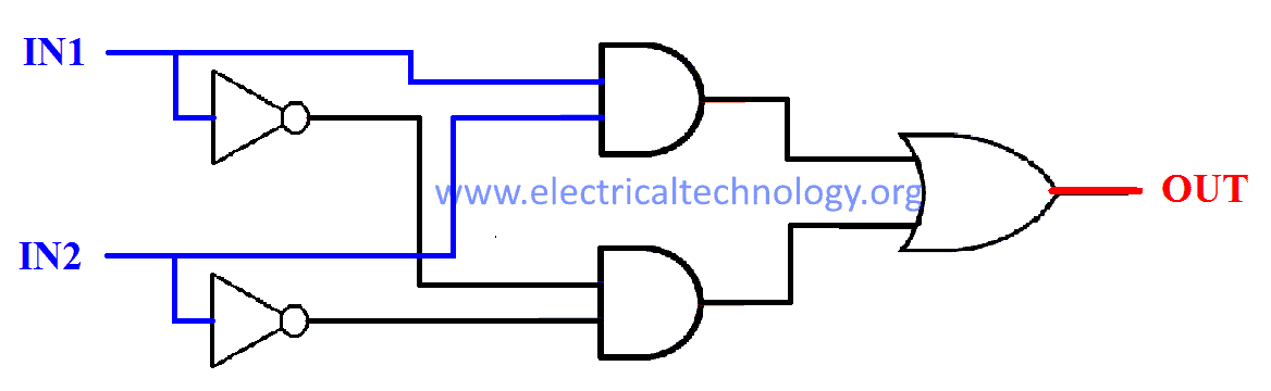
OUT = ( I̅N̅1̅ & I̅N̅2̅) + (IN1 & IN2) Expression 1
OUT = (IN1 + IN2)’ + (IN1&IN2) Expression 2 DE MORGAN’S LAW
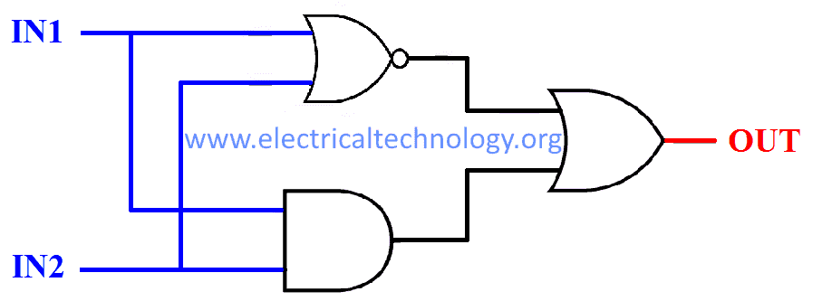
Using NOT, AND & OR Gate
Expression 1 can be implemented with NOT, AND, OR gates as shown in the figure given below.
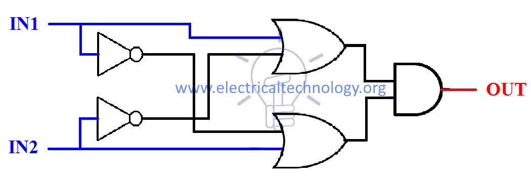
Using NOR, AND & OR Gate
Expression 2 uses NOR, AND & OR gate to reduce the number of used gates as shown in the figure given below.
Product of Sum
In this expression, we use the product of Max terms. Max terms are the sum of inputs for which output is LOW state “0”.
POS expression can be easily implemented with NOR gates.
According to the truth table given above the POS (product of sum) expression is :
OUT = (I̅N̅1̅ + IN2) & (IN1 + I̅N̅2̅) Expression 1
This expression can be implemented with NOT, AND, OR gates as shown in the figure given below.
 XNOR Gate From Universal Gates
Universal gates are those gates which can be implemented into any logic gate or logic function.
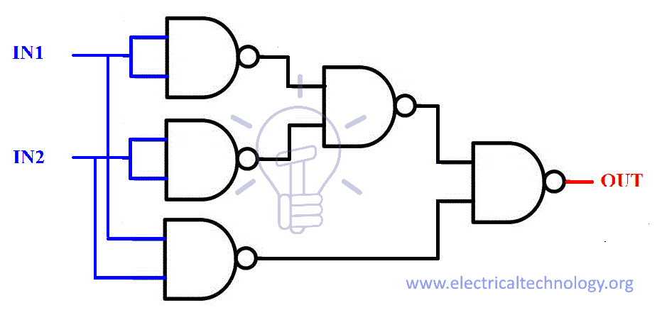
XNOR Gate From NAND Gate
NAND gate is a universal gate. It can be implemented into any Logic function.
As we have discussed before SOP (sum of product) expression can be easily implemented with NAND gates, so SOP expression for XNOR gate is
OUT = { (I̅N̅1̅ & I̅N̅2̅) + (IN1 & IN2) }
OUT’ = { (I̅N̅1̅ & I̅N̅2̅) + (IN1 & IN2) }’ Taking complement on both sides
OUT’ = { (I̅N̅1̅ & I̅N̅2̅)’ & (IN1 & IN2)’ } De Morgan’s Law
OUT’’ = { (I̅N̅1̅ & I̅N̅2̅)’ & (IN1 & IN2)’ }’ Taking complement on both sides
OUT = [ { (IN1 & IN1)’& (IN2 & IN2)’ }’ & (IN1 & IN2)’]’ (IN1 & IN1)’ = I̅N̅1̅
Now, this expression is in NAND form. And can easily be implemented with NAND gates as shown in the figure below.
XNOR Gate From NOR GATE
NOR gate is also a universal gate. It can be implemented into any Logic function.
As we have discussed before POS (product of sum) expression can be easily implemented with NOR gates, so POS expression for XNOR gate is given below
OUT = { (I̅N̅1̅ + IN2) & (IN1 + I̅N̅2̅) }
OUT’ = { (I̅N̅1̅ + IN2) & (IN1 + I̅N̅2̅) }’ Taking complement on both sides
OUT’ = { (I̅N̅1̅ + IN2)’ + (IN1 + I̅N̅2̅)’ } De Morgan’s Law
OUT’’ = { (I̅N̅1̅ + IN2)’ + (IN1 + I̅N̅2̅)’ }’ Taking complement on both sides
OUT = [ { (IN1 + IN1)’+ IN2}’ + { IN1 + (IN2 + IN2) }’ ]’ (IN1 + IN1)’ = I̅N̅1̅
Now, this expression is in NOR form. And can easily be implemented with NOR gates as shown in the figure below.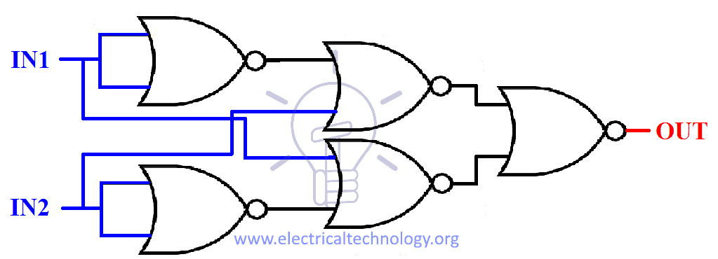
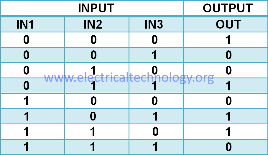
Multi-Input Exclusive NOR Gate
XNOR gate gives HIGH state “1” only when there is an even number of HIGH state “1” inputs.
XNOR gate can have more than two inputs but it has only one output.
Truth Table
The truth table of “3” inputs XNOR gate is given below.
Construction:
Combinational Logic
Combinational logic is the logic of making a schematic with the help of basic logic gates.
Sum of products (SOP) and products of the sum (POS) are two methods in combinational logic.
Sum of Products
SOP uses the idea of summation of min terms (product of inputs for which output is high)
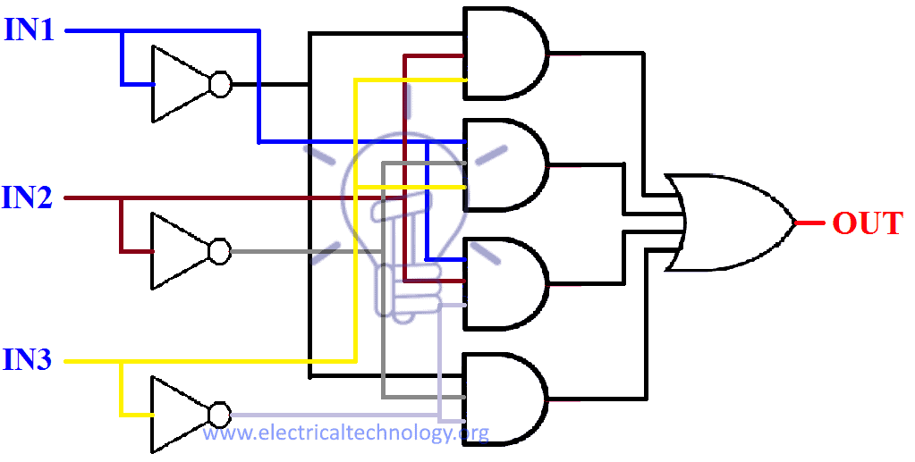
According to the truth table given above, Sum of product expression and schematic for 3-input XNOR gate is given below.
OUT = (I̅N̅1̅ & I̅N̅2̅ & I̅N̅3̅) + (I̅N̅1̅ & IN2 & IN3) + (IN1 & I̅N̅2̅ & IN3) + (IN1 & IN2 & I̅N̅3̅)
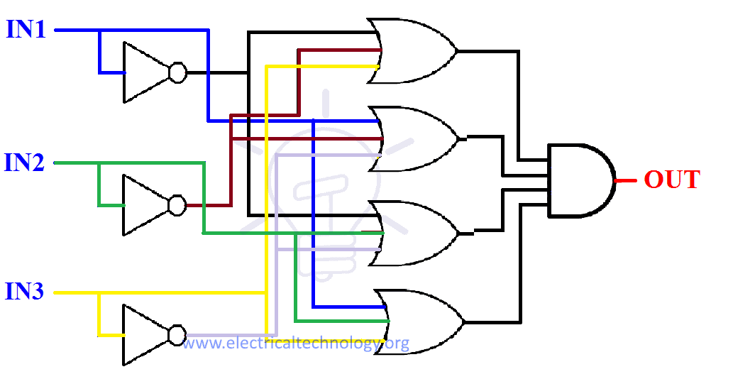
Product of Sum
POS uses the idea of product of max terms (Sum of inputs for which output is LOW.)
According to the truth table given above, Product of sum expression and schematic for 3-input XNOR gate is given below.
OUT = (I̅N̅1̅ + I̅N̅2̅ + IN3) & (I̅N̅1̅ + IN2 + I̅N̅3̅)& (IN1 + I̅N̅2̅ + I̅N̅3̅) & (IN1+ IN2+ IN3)
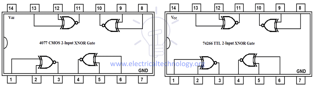
TTL and CMOS Logic XNOR Gate IC’s
Some of XNOR ICs with pin configurations is given below.
TTL Logic XNOR Gate
- 74266 Quad 2-input (with open collector outputs)
- 747266 Quad 2-inout
CMOS Logic XNOR Gate
- 4077 Quad 2-Input
4077 CMOS and 74266 TTL XNOR Gate IC (Quad 2-Input)
Pinout for 74266 TTL XNOR Gate IC
| PIN Number | Description |
| 1 | Input Gate 1 |
| 2 | Input Gate 1 |
| 3 | Output Gate 1 |
| 4 | Output Gate 2 |
| 5 | Input Gate 2 |
| 6 | Input Gate 2 |
| 7 | Ground |
| 8 | Input Gate 3 |
| 9 | Input Gate 3 |
| 10 | Output Gate 3 |
| 11 | Input Gate 4 |
| 12 | Input Gate 4 |
| 13 | Output Gate 4 |
| 14 | Positive Supply Voltage |
Exclusive NOR Gate Applications
Some common application and uses of XNOR or Exclusive-NOR gate are as follow:
- It is used in error detecting circuits to detect odd/even parity bits in digital transmission circuits.
- Also used in encryption and arithmetic circuits as a combination of XNOR zand XOR circuit for low power consumption
- Also used in security or quantity measuring circuits such as in heat exchanger tank to ring the alarm when the heat or temperature goes up/down.
- In calculators, computers and digital logic circuits.
You may also read more about Digital Logic gates
Logic NOT Gate – Digital Inverter Logic Gate Digital Logic OR Gate Digital Logic AND Gate Digital Logic NOR Gate