Digital Logic OR Gate
Digital Logic OR Gate – Digital Gates
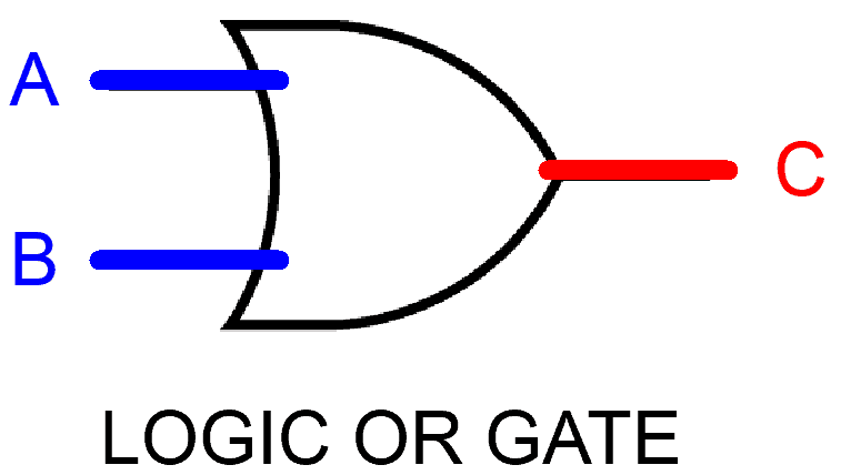
What is Logic OR Gate
A logic gate which gives low state “0” only and only when all of the inputs are low state “0”. Otherwise, provide high state “1” as output.
Logical OR gate can have 2 or more than 2 input lines but it has one output line. It can be either true or false, true being High state”1” and false being Low state”0”.
OR Gate works on submission bases. i.e.
If either “A” or “B” is “1”, Then “C” is 1.
Good to know: These terms also used in binary logic gates and circuits 0 or 1 Low or High True or False ON or OFF
OR Gate Logic Symbol, Boolean Expression & Truth Table
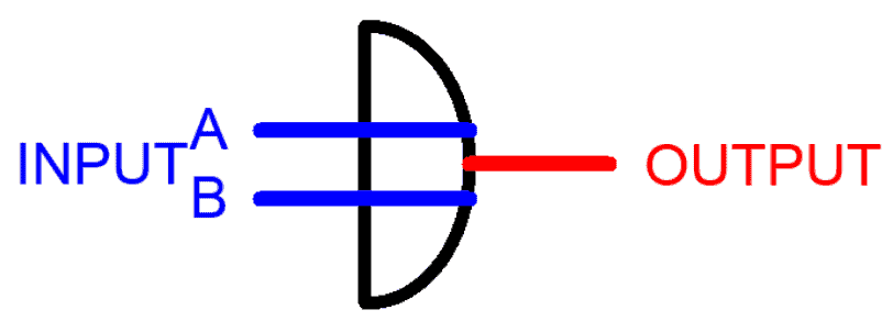
OR Gate Symbol
There are 3 types of symbols used for OR gate all over the world.
American National Standards Institute (ANSI) MILITARY

International Electrotechnical Commission (IEC) EUROPEAN

Deutsches Institut für Normung (DIN) GERMANY
Boolean Expression
In Boolean algebra (+) sign is used for OR operation, which gives high state “1” if either one or both of the operands are a high state. In most of the programming languages (|) is used for Bit wise OR operation while (||) is used for logical OR operation.
C = A+B, C=A|B, C=A || B,
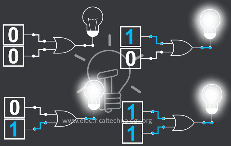
Truth Table
A mathematical table used to specify input to output logic combination of a digital circuit is known as a truth table, the truth table of OR Gate is given below.

OR Gate Logic Flow Schematic Diagram
Construction and Working Mechanism of OR Gate
OR Gate using Resistor – Diode Logic
In resistor-diode logic (RDL), the diode is used as a switching unit. In the schematic given below RDL logic OR gate is given, in which 2 diodes and 1 pull down resistor are used. Pull down resistor means that whenever the diodes are in reversed bias it will pull output voltages down to 0 volts (LOW state “0”).
Diodes are used in a parallel configuration. When both of the input A and B are “0”, diodes will be reverse bias meaning no current will flow; as a result, output volts will be pulled down i.e. LOW STATE “0”. And if there is even a single high state input, then its corresponding diode will become forward bias resulting in high state “1” flow out as output. Hence resulting in the truth table given below.
There is also 0.7 volts drop in the diode.

OR Gate using Resistor – Transistor Logic
In Resistor-Transistor logic (RTL), Bipolar Junction Transistor (BJT) is used as a switching unit. BJTs are high power consumption devices as it operates on base current. RTL logic schematic of OR gate is given in the figure given below. In this schematic two NPN transistor is used in parallel configuration and 2 input resistors and a pull-down resistor.
There are two discrete input lines connected with separate NPN transistor’s base. And an output line is taken between resistor and NPN Transistors.
NPN transistors switch on when there is a HIGH input at its base and current starts flowing through the transistor.
When both of the inputs are LOW state “0”, BJTs will be switched off, as a result, there will be no current flow and OUTPUT “C” will be pulled down to “0 LOW state”.
When there is a single HIGH state input, one of the BJTs connected in parallel will turn on and start conducting current and eventually producing voltage Vcc “high state 1” across load resistor “R” which is taken as OUTPUT C.
The truth table of the described schematic is given below.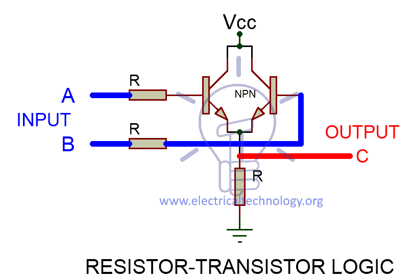
OR Gate using MOS Logic
In MOS logic, the main switching units are MOSFETs, MOSFETs are fast switching, low power consumption devices as it operates on gate voltages, MOS logic schematic of OR gate is given in the figure below.
MOS logic uses the same working principle as RTL logic, the only difference is use MOSFETs instead of BJTs. As you can see in the figure given below inputs are fed through the input resistor to the gates of two parallel connected NMOSFETs and output is taken across load resistor “R1”.
NMOSFETs switch on when there is high state “1” on its gate and starts conducting current through it. And turns off when there is LOW state and become open(no flow of current).
When both input lines are LOW state “0”, both NMOSFETs will be switched off and there will be no current flow. So the only path connected to output will be GND (LOW state 0).
If there is a single high state input or both of the inputs are a high state then one or both of the NMOSFETs will be switched on respectively. It will give a closed path for current to flow through Vdd to GND. As a result, there will be a voltage drop across LOAD resistor resulting in HIGH state “1” at the output.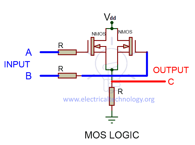
OR Gate From Other Logic Gates
OR gate functionality can be achieved with the help different combinations of the different logic gate. Some of them are given below;
NAND and NOR gates are Universal gates which can be used to implement any kind of Boolean function. It’s very easy to implement,
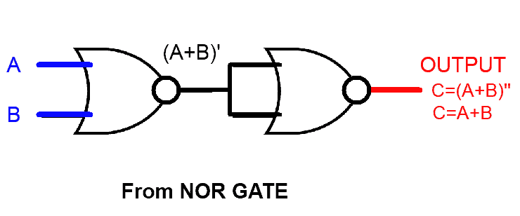
OR Gate constructed from NOR Gate
OR Gate from NAND Gate

OR Gate from NOR, NOT Gate
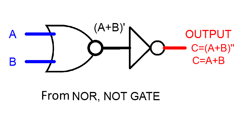
OR gate constructed from NOR GATE is given above. NOR is actually INVERT of OR. So placing an INVERT/NOT gate to the output of NOR gate will provide OR gate’s result. Or placing a NOR gate with common input line in front of NOR gate will also do the job as it will act as an INVERTER.
NAND gates operation is same as AND gate but with an inverted output. So feeding it inverted input will provide the Operation OR as explained in below Boolean expressions
C = (A + B) Taking complement on both side
C’= (A + B)’ De Morgan’s law
C’= (A’ . B’) Taking complement again on both side
C= ( A’ . B’)’
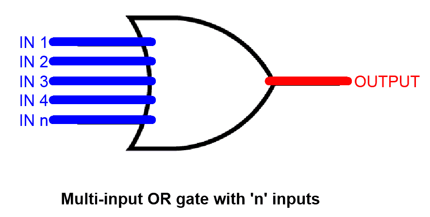
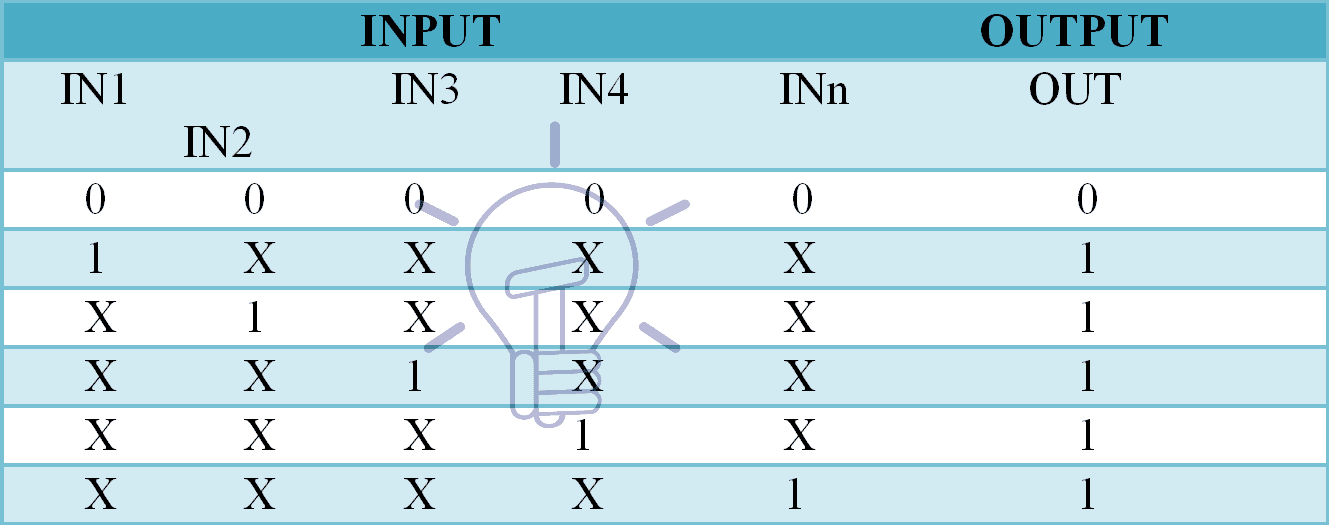
OR Gate with Multiple Input
OR gate can have more than 2 inputs and can be used according to the requirements of the schematic design.
OR gate with “n” number of input is given below.
Truth Table
NOTE: In the table given below “X” means “don’t care”. It can be “1”and it can be “0”. Which means, as long as there is a single input carrying “1”, the output will be always “1” so there is no reason to put a check on other inputs, that’s why it’s called “don’t care X”.
Resistor-Diode Logic
IN RDL (Resistor-Diode logic) logic, a diode is used on every input line, thus adding diodes can potentially increase the number of input lines as shown in the figure below. Each input is fed to separate diode. Place as many diodes as you would like, to create a Multi-Input RDL OR GATE.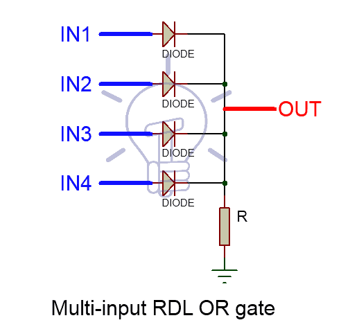
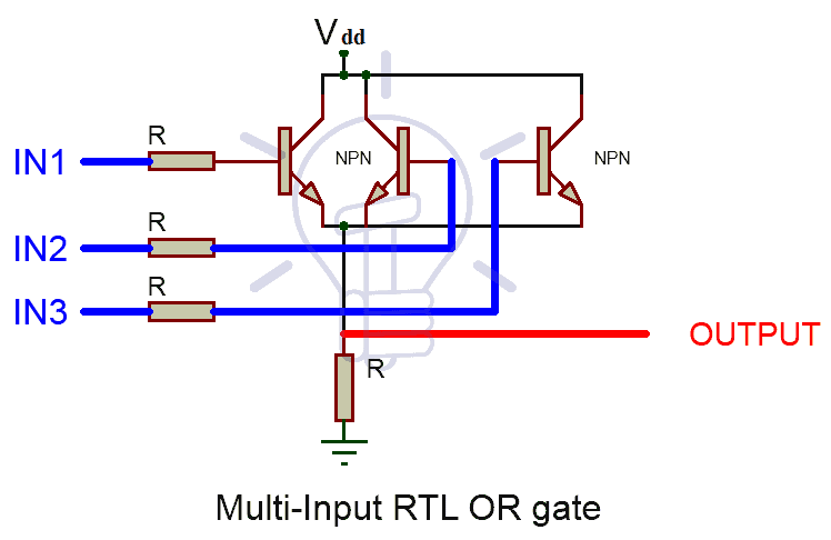
Resistor-Transistor Logic
In RTL (Resistor-Transistor Logic), Transistors are used as switching unit. To increase the input lines we have to increase the number of transistors connected in parallel as shown in the figure below.
MOS Logic
The idea to create a Multi-Input OR gate in MOS logic is exactly same as in RTL logic. Increasing the number of MOSFETs in parallel can potentially increase the number of input lines. The figure given below shows MOS logic OR gate schematic.
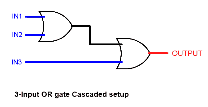
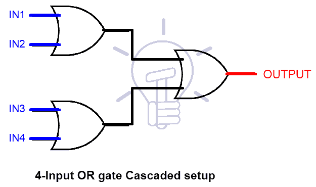
By Cascading 2-input gates
Multi-input OR gate can be made from cascading setup of 2-input OR gates as shown in the figure given below.
OUT = IN1 + IN2 + IN3
OUT = (IN1 + IN2) + IN3
OUT = IN1 + IN2 + IN3 + IN4
OUT = (IN1 + IN2) + (IN3 + IN4)
TTL and CMOS Logic OR Gate IC’s
Commercially up to 4-Input OR gate IC’s are available in the market, having two OR gates in a single package.
Such as:
TTL Logic OR Gates
- 74LS32 Quad 2-input OR Gate
- 744075 TTL 3-Input OR Gate
CMOS Logic OR Gate
- CD4071 Quad 2-input OR Gate
- CD4075 Triple 3-input CMOS OR Gate
- CD4072 Dual 4-input CMOS OR Gate
Hex 2-input OR drivers
- 74832
4071 CMOS and 7432 TTL OR Gate IC (2-Input)
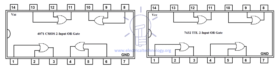
Pinout for 7432 TTL OR Gate IC
| PIN Number | Description |
| 1 | Input Gate 1 |
| 2 | Input Gate 1 |
| 3 | Output Gate 1 |
| 4 | Input Gate 2 |
| 5 | Input Gate 2 |
| 6 | Output Gate 2 |
| 7 | Ground |
| 8 | Output Gate 3 |
| 9 | Input Gate 3 |
| 10 | Input Gate 3 |
| 11 | Output Gate 4 |
| 12 | Input Gate 4 |
| 13 | Input Gate 4 |
| 14 | Positive Supply |
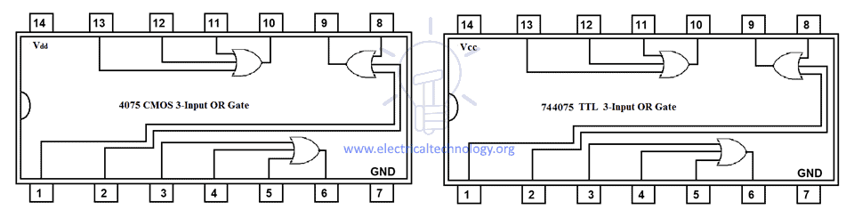
4075 CMOS and 744075 TTL OR Gate IC (3-Input)
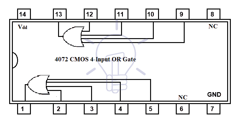
4072 CMOS OR Gate IC (4-Inout)
Commonly available OR Logic Gate IC are given in the table below:
| 4071 | Quad 2-Input OR Gate |
| 4072 | Dual 4-Input OR Gate |
| 4073 | Triple 3-Input AND Gate |
| 4075 | Triple 3-Input OR Gate |
| 7432 | Quad 2-Input OR Gate |
| 741G32 | Single 2-Input OR Gate |
| 741G86 | Single 2-Inout Exclusive OR Gate |
| 74832 | Hex 2-Input OR Drivers |
| 741G3208 | Single 3-Input OR-AND Gate |
| 744075 | Single 3-Inpout OR Gate |
| 744078 | 8-input OR / NOR Gate |
OR Gate Applications
OR Gate has been widely used in practical life applications such as:
- To detect exceed of specific quantities / parameters (such as temperature or pressure) and produce command signal for the system to take required action.
- Alarm circuit for car door system
- In calculators, computers and digital logic circuits.
You may also read more about Digital Logic gates
Logic NOT Gate – Digital Inverter Logic Gate Exclusive-NOR (XNOR) Digital Logic Gate Digital Logic AND Gate Digital Logic NOR Gate


I am confused of notation of OR in boolean algebra. Here it says + is OR gate, but when I search it up, for example in wikipedia, it says + is actually a XOR gate. Which is correct?
“+” as a summation used for OR Gate.
You can compare the four logic gates as follow. It will clear the basic concept.
Digital Logic OR Gate
Digital Logic NOR Gate
Digital Logic XOR Gate
Digital Logic XNOR Gate