What is MEMS – Microelectromechanical Systems Technology ?
A Introduction to Microelectromechanical Systems (MEMS) Technology
Let us define MEMS!
MEMS stands for Micro-Electro-Mechanical System, an integrated system of mechanical and electro-mechanical devices and structures, manufactured using micro fabrication techniques. A MEMs device consists of 3 dimensional properties which sense and manipulate any physical or chemical property. Basic components using micro sensors, micro actuators and other micro structures, which are fabricated on a single silicon substrate. 
Like a typical mechatronics system, a MEMS device constitutes of a micro sensor to sense a particular variable of the environment and converts the variable to an electrical signal. This electrical signal is processed by microelectronics which accordingly controls a micro-actuator to produce the required change in environment.
- You may also read: What is WiMAX? Difference between Broadband WiMax and WiFi
What is MEMS constituted of?
Like said above, basic components of a MEMs device include micro-sensors and micro-actuators, which convert one form of energy to another. A MEMs device can have static or movable components, whose physical dimension varies from below one micron, to, above several millimetres. While a micro-sensor converts measured mechanical signal (i.e. physical or chemical parameter) to electrical signal, a micro-actuator does vice versa.
Different types of micro-sensors are available for almost every measurable parameter like temperature, pressure, smell, magnetic fields, radiation, speed, acceleration etc. It is noteworthy that for the past few years, performance of these micro-sensors have surpassed that of their macro scale versions along with other benefits like low production cost.
Different varieties of micro-actuators include micro-valves to control flow, optical switches and mirrors to control light beams, micro-resonators, micro-pumps to develop positive fluid pressure.
- You may also read: What is Automated Fingerprint Identification System and How it Works?
Ways of Fabrication of MEMS??
Fabrication of MEMs devices is done using conventional integrated circuit fabrication techniques like lithography, deposition, etching along with different micro-machining techniques. While the conventional techniques are used to obtain two dimensional structures, the micro-machining techniques enable extension to three-dimensional structure.
All MEMs or micro-fabrication device fabrication commences with growth of thin, flat material known as substrate, on which the whole structure is created. While crystalline silicon, owing to its low cost and high availability is the foremost choice for MEMs substrate, other materials like quartz, glass, ceramics, polymers are also used.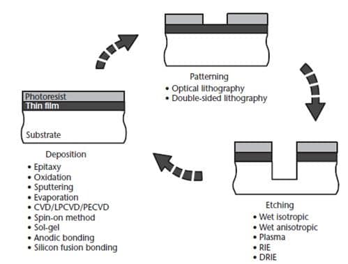 Prior to micromachining, let us get a brief idea about the two basic processes.
1. Deposition: This involves deposition of thin film of materials on silicon substrate. Two varieties of deposition are as given below:
2. Chemical Deposition: This involves creation of solid materials from chemical reactions in gas and/or liquid compositions, either directly or with the substrate material. Types include Thermal Growth (Silicon Dioxide grown on Silicon at temperature range from 750 to 1200 degree Celsius.), Chemical Vapour Deposition (Solid material formed on the substrate as a result of chemical reaction between ambient gases), electro-deposition (formation of solid material by electrical conductivity) and Epitaxy.
3. Physical Deposition: This involves physically moving the substance to be deposited on the substrate. Types include Physical Vapour Deposition (Deposition of material by condensation of vapours of the source material) and Casting (Deposition of material dissolved in liquid solvent, by spraying or spinning).
4. Lithography: It involves formation of patterns on a chemically resistant polymer which is deposited on the substrate. These patterns are then transferred to the base or substrate layer accordingly.
Types include Photolithography (A transparent photomask coated with opaque pattern is placed in contact with the photo sensitive material deposited on the substrate, is exposed to radiation of a particular wavelength, causing either strengthening or weakening of the photoresist and transferring of the pattern to the organic layer), Double Sided Lithography and Gray Scale Lithography.
Typical micromachining techniques include bulk micromachining, where structures are etched into the silicon substrate, and surface micromachining, where micro-mechanical layers are formed by deposition on the surface. Other techniques like silicon wafer bonding, LIGA and 3-D microfabrication are also used for high aspect ratio structures.
- You may also read: An Overview of RFID Based Library Management System
-
Bulk Micromachining:
As the name suggests, it involves selective etching of bulk of silicon wafer to realize micro-mechanical structure. Etching can be Wet Etching or Dry Etching. Wet Etching involves etching of the material by dissolving it in a chemical etchant solution like HNA (Hydrofluoric acid, Nitric Acid and Acetic Acid), Potassium Hydroxide (KOH).It can be anisotropic etching (selective etching in specific direction) or isotropic etching (uniform etching in all directions).

Dry Etching can be classified as Reactive Ion Etching (RIE) (where Radio Frequency (RF) energy is used to energise a plasma of reactive gases, to form ions which can cause either chemical or physical etching), Sputter Etching (where the material or Silicon wafer is subjected to ion bombardment) and Vapour Phase Etching (Silicon Wafer is placed in a chamber full of gases, wherein the deposited material is dissolved in a chemical reaction).
Commonly used technique for MEMS device is Deep Reactive Ion Etching (DRIE), modified Reactive Ion Etching technique where higher aspect ratios can be achieved by selective etching on the horizontal surface and not on the sidewalls.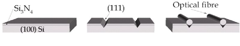
- You may also read: What is ZigBee Technology and How it works?
-
Surface Micromachining:
It involves using the substrate as a foundation block on which processing can be done. Thin film layers are added as structural layer (on which a free standing structure is made) and sacrificial layer (which is required for lithography and etching). Silicon Oxide is the commonly used sacrificial layer, whereas Polysilicon is the commonly used structural layer.

3. High Aspect Ratio Micromachining:
It involves combing the micromachining with other techniques like injection moulding and electroplating. Commonly used technique is LIGA (Lithography, Electroforming and Moulding). Here, titanium, Copper or Aluminium layer is deposited on the substrate to form a patter and Nickel is coated over it to form the base plate.

An X-Ray sensitive material like PMMA is then added to the substrate. The whole structure is subjected to X-Ray radiation where the exposed areas of PMMA are dissolved, thus electroforming the metal. The end products can be used as a final product or can be used as an injection tool.
- You may also read: What is Internet of Things (IOT) and Its Applications in Electrical Power Industry
Application Areas of MEMS Technology
1. Automotive Industry: Examples of MEMS devices include internal navigation sensors, airbag sensors, Air conditioning compressor sensors, fuel level and vapour pressure sensors etc.
2. Electronics Industry: Examples include inkjet printer heads, disk drive heads, earthquake sensors, mass data storage systems etc.
3. Medical Industry: Examples include Pacemakers, Prosthetics, Blood pressure sensors etc.
4. Defence: Examples are arming systems, munitions guidance, surveillance etc.
5. Communications: Examples are fibre optic components, voltage controlled oscillators, tuneable lasers, splitters and couplers etc.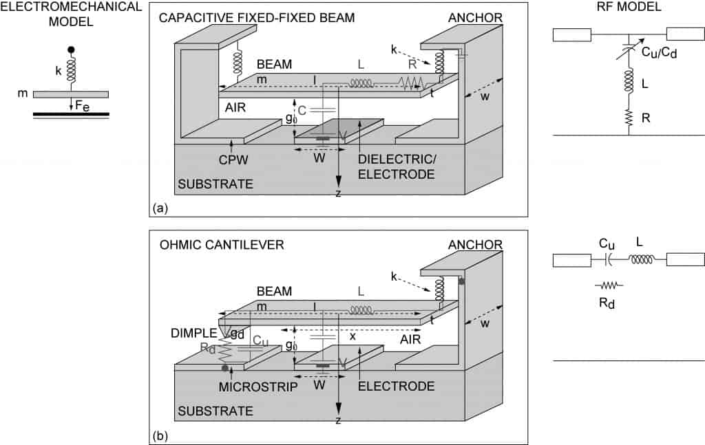
Future with MEMS!
While the simplest form of MEMS structure involves a single discrete micro-sensor, micro-actuator integrated with electronics, the practical applications require complex forms of MEMS devices which is possible by complex integration of MEMS with other techniques like Nanotechnology, Photonics etc.
Actually this vision of integration of all these technologies on a single chip is sought to be the most promising technological breakthrough in the future. Another form of integration which seems to be fruitful is integration with Biomedical science and optoelectronics.
It is noteworthy that from the past few years, highly innovative products have emerged from the integration of Biomedical science with MEMS, enabling revolutionary applications like DNA sequencing, water and environmental monitoring, drug discovery etc. Also integration of MEMS with optical communications have resulted in achieving practical means to curb ongoing network scaling issues.
Also in recent times, with evolution of Internet Over Things (IOT) market (smart devices), requirement of MEMS sensors has increased manifold. Also these smart systems cannot be just limited to Silicon based technologies, but rather Polymer based technologies.
So this is a brief yet significant information regarding MEMS, though there are many other things yet to be discussed, like the hiccups in this technology and of course some practical examples. Readers are invited to add in to these two points.
- You may also read: What is PID Controller & How it Works?


This is a detailed article. As someone coming from Instrumentation background, this was a very helpful post.