Digital Logic NAND Gate – Universal Gate
Universal Digital Logic NAND Gate
What is Logic NAND Gate?
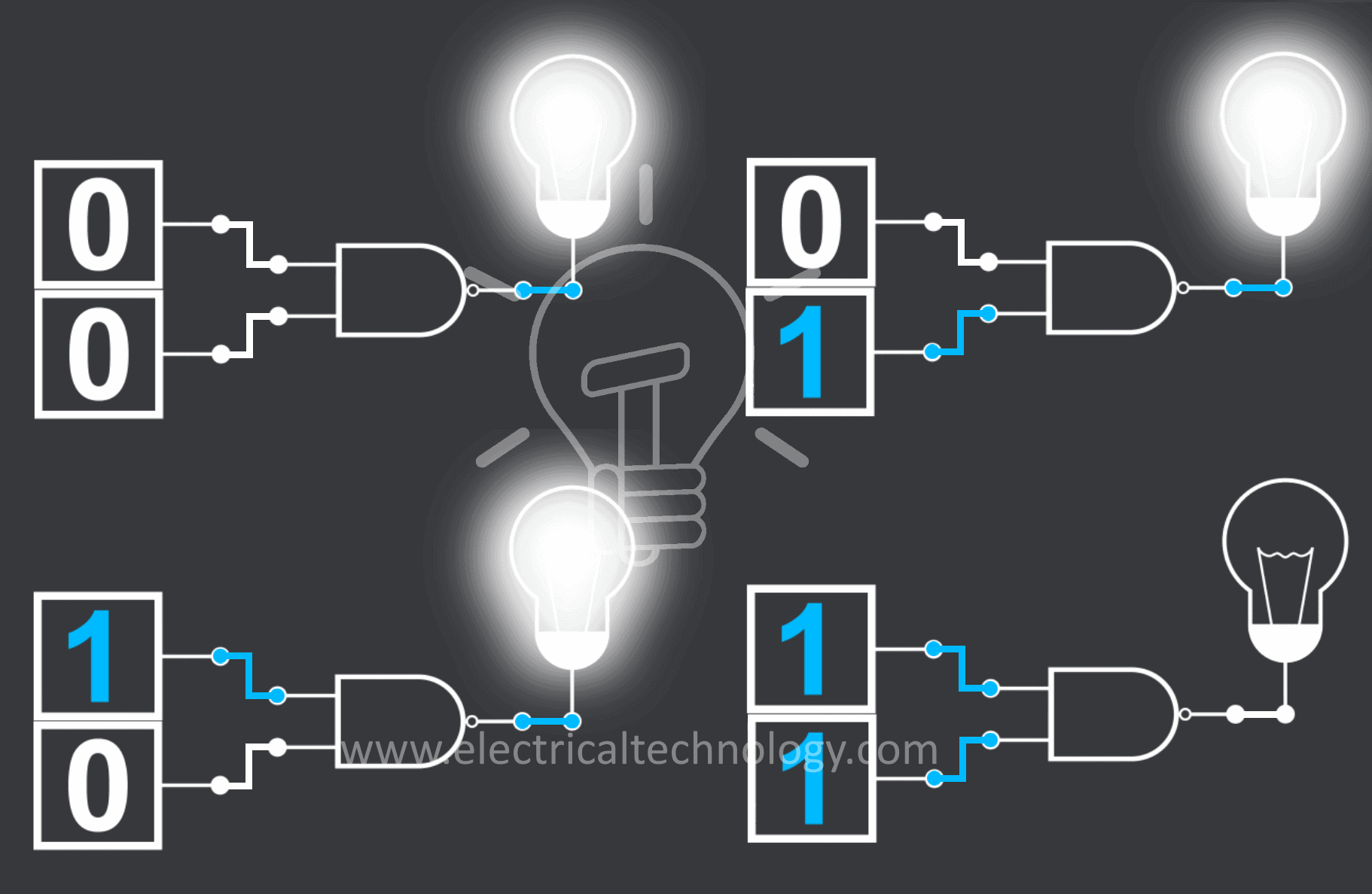
NAND Gate is a digital logic gate (Also known as Universal gate) produces logic LOW State “0” only and only when there is HIGH State “1” at all of the inputs.
NAND gate is opposite /Invert of AND gate, in other words, if we connect NOT gate to the output of AND gate it will become NAND gate.
Usually, NAND gate has two inputs and 1 output but it can have as many inputs as you want according to your design. It is the reversal of AND Gate.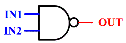
NAND Gate Logic Symbol, Boolean Expression & Truth Table
NAND Gate Symbol
There are 3 types of symbols used for NAND gate all over the world.
American National Standards Institute (ANSI)/ MILITARY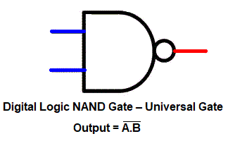
International Electrotechnical Commission (IEC)/EUROPEAN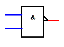
Deutsches Institut für Normung (DIN)/GERMANY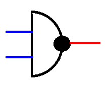
Boolean Expression
OUT = (IN1 . IN2)’ or OUT = (IN1 & IN2’)
or ![]()
Truth Table
NAND Gate Logic Flow Schematic Diagram
Digital Flip-Flops – Types & Operation of Flip-Flops
NAND Gate Construction And Working Mechanism
Resistor-Transistor Logic (RTL)
In Resistor-Transistor logic (RTL), Bipolar junction transistors (BJTs) are used as switching unit. NAND gate schematic in RTL logic is given in the figure below.
In this schematic two NPN BJTs are used in the series configuration.
NPN transistors are active high, which means they will turn on when there is high state “1” at its base input and it will start conducting current. When there is logic LOW state “0” input then it will turn-off.
According to this schematic, when there is logic HIGH state “1” at both input lines, the transistor will switch on and the path from GND to output will be complete, thus resulting in logic LOW state “0” output.
When there is logic LOW state “0” at any or both input lines, then the NPN (one or both) will switch-off, cutting the path to the output and the only path remaining will be Vcc to output. Which will result in logic HIGH state “1” at output.
The truth table of the described schematic is given below.
![]()

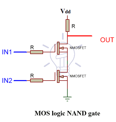
MOS Logic
In MOS logic, MOSFETs are used as the main switching unit.
Contrary to RTL logic, MOS logic uses MOSFETs instead of BJTs. MOS logic schematic of NAND gate is given below.
NMOSFET is active high, which means it switch-on when there is high state input at its gate and it starts conducting current. And its witches off when its gate input is logic LOW state “0”.
According to this schematic, when there is HIGH state “1” at its both input lines, these both NMOSFETs will switch on, resulting in creating a path from GND to output. Which will result in logic LOW state “0” as output.
When there is a single logic LOW state “0” at its input or both of the inputs are logic LOW state “0” then the NMOSFETs will switch off, resulting in breaking the path from GND to output. And the only path that remains will be the Vdd to output. So the output will become logic HIGH state “1”.
the Truth table of the following design is also given below.
NAND Gate From Other Gates
NAND gate function can be achieved with the combination other gates. Some of them are given below.
- Invert of AND gate is NAND gate. Thus connecting a NOT gate to the output of AND gate will result in NAND gate as shown in the figure.

- NOR is a universal gate i.e. It can be made into NAND gate with specific configuration given in the figure below.

NAND Gate is a Universal Gate. The universal gate is a gate which can be implemented into any other logic gate or logic function. Some of the basic gate‘s implementations are given below.
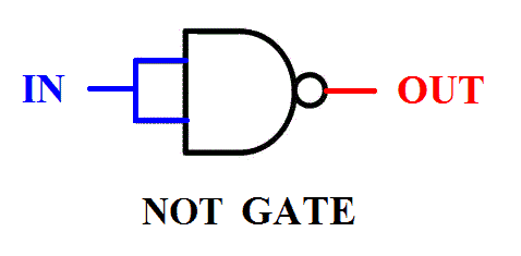
NAND from NOT Gate
NAND gate can be used as NOT gate if we combine its input together into a single input.
In NAND gate all high state inputs lead to LOW output, and all LOW state inputs lead to HIGH input, Which is exactly the same as a NOT gate. NOT gate implementation from NAND gate diagram is given below.
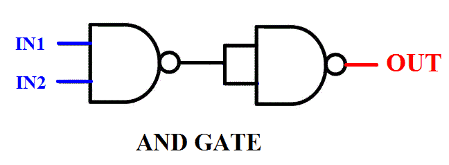
NAND from AND Gate
NAND gate is opposite/invert of AND gate and vice versa. So inverting output of NAND gate will result in AND gate. To invert NAND gate‘s output, we have to use NAND gate with combined inputs which work as Inverter/NOT gate. The figure of implementation of AND gate from NAND gates is given below.
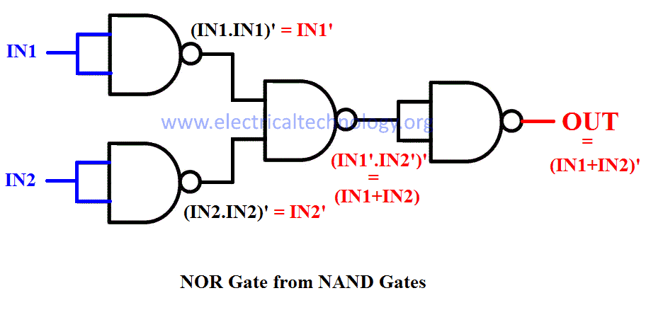
NAND from OR Gate
To better understand the implementation of OR gate using NAND gate one need to know about Boolean algebra and De Morgans law.
Conversion of NAND to OR gate Boolean Algebraic expression is given below.
OUT = (IN1 + IN2)
OUT‘ = (IN1 + IN2)‘ taking complement on both sides.
OUT‘ = (IN1‘&IN2‘) De Morgans law
OUT‘‘ = (IN1‘&IN2‘)‘ taking complement on both sides.
OUT = {(IN1&IN1)‘&(IN2‘&IN2‘)}‘ IN1= (IN1&IN1)
So the end result is in the form of NAND gate. As you can see IN1,IN2is NAND (operation) with themselves and then they are NAND (operation) with each other. To better understand observe the figure given below.

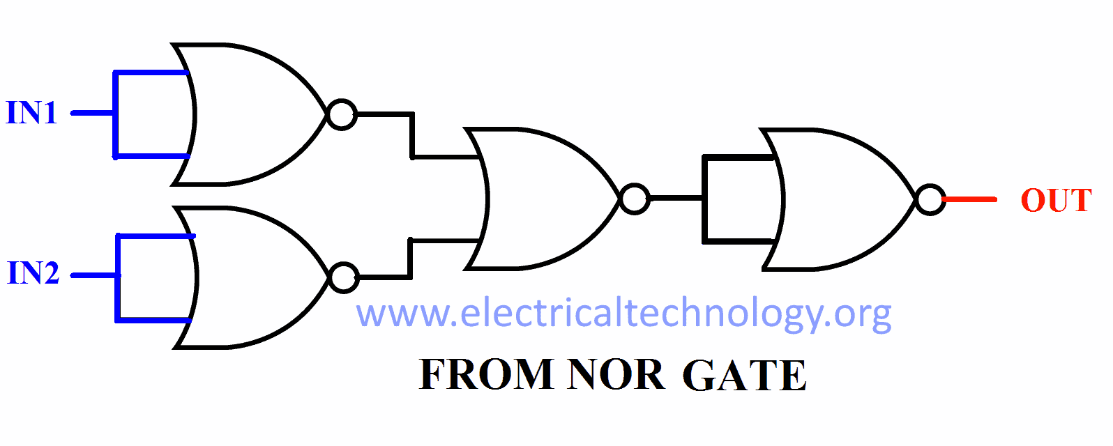
NAND from NOR GATE
NOR gate is invert of ORgate.OR gate design will be the same as illustrated above. There will be an Inverter/NOT gate at the output of OR gate as shown in the figure given below.
Multiple Input NAND Gate
As we have established before that NAND gate’s output will be logic LOW state “0” only and only when there is logic HIGH state “1” at its all input lines.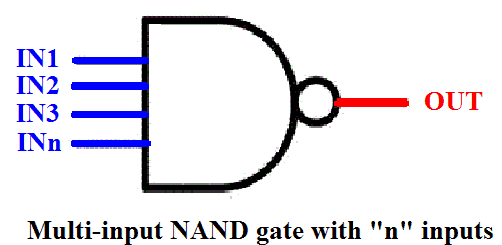
Multiple Input NAND Gate Truth Table
NAND gate truth table with ‘n’ inputs is given below.
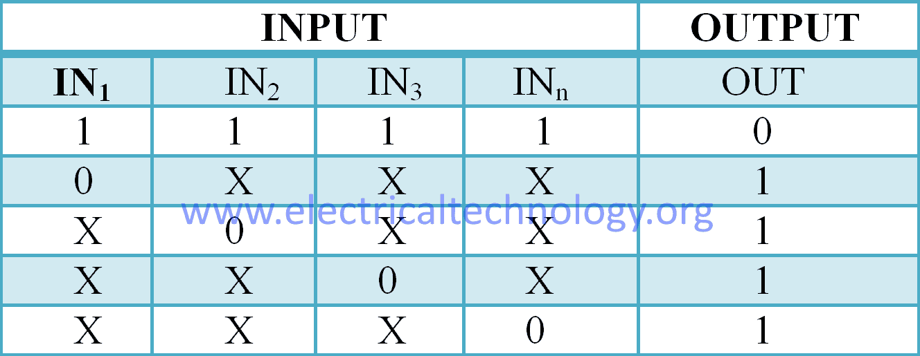
NOTE: In the table given above “X” means “don’t care”. It can be “1”and it can be “0”. Which means, as long as there is a single input carrying “0”, the output will be always “1” so there is no reason to put a check on other inputs, that’s why it’s called “don’t care X”.
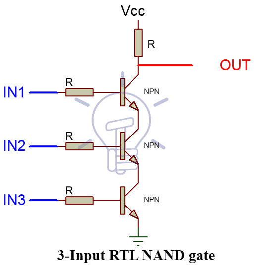
RTL
As you know, BJTs are the switching unit in RTL and they are connected with separate input lines. Hence connecting another NPN BJT in the series configuration can increase the input lines.
A 3-input NAND gate schematic in RTL is shown in the figure given below.
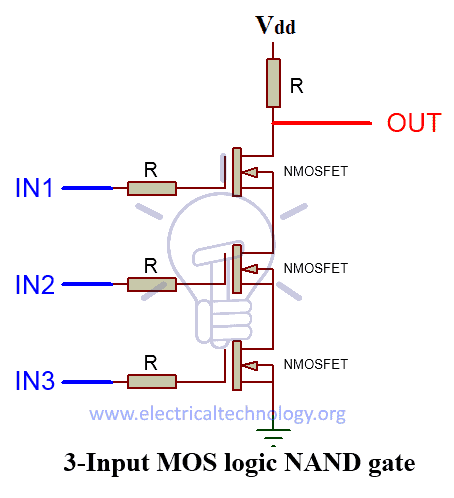
MOS Logic
In MOS logic, input lines are directly connected with NMOSFETs, So increasing the number of NMOSFETs connected in series can potentially increase the number of input lines.
A 3-input NAND gate schematic in MOS logic is given below.
From Cascading NAND Gates
Multi-Input NAND gate can be made from cascade setup of 2-input NAND gates.
OUT = (IN1&IN2& IN3)‘
OUT = ((IN1&IN2)’’ & IN3)’
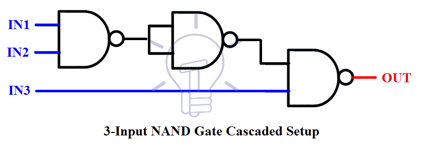
Since (IN1&IN2)‘‘ = (IN1&IN2)
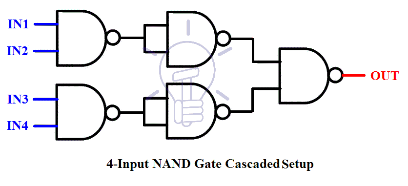
OUT = (IN1& IN2& IN3& IN4)’
OUT = ((IN1&IN2)’’ & (IN3& IN4)’’)’
TTL and CMOS Logic NAND Gate IC’s
Commercially up to 8-input NAND gate’s IC are available in the market. Some of the commonly used IC’s details are given below.
TTL Logic NAND Gates
- 74LS00 Quad 2-input
- 74LS10 Triple 3-input
- 74LS20 Dual 4-input
- 74LS30 Single 8-Input
CMOS Logic NAND Gates
- CD4011 Quad 2-input
- CD4023 Triple 3-input
- CD4012 Dual 4-input
4011 CMOS and 7400 TTL NAND Gate IC (Two-Inputs)
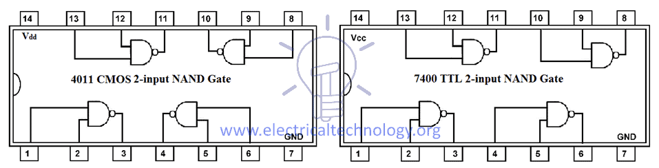
Pinout for 7400 TTL NOR Gate IC
| PIN Number | Description |
| 1 | Input Gate 1 |
| 2 | Input Gate 1 |
| 3 | Output Gate 1 |
| 4 | Input Gate 2 |
| 5 | Input Gate 2 |
| 6 | Output Gate 2 |
| 7 | Ground |
| 8 | Output Gate 3 |
| 9 | Input Gate 3 |
| 10 | Input Gate 3 |
| 11 | Output Gate 4 |
| 12 | Input Gate 4 |
| 13 | Input Gate 4 |
| 14 | Positive Supply Voltage VCC |
4023 CMOS and 7410 TTL NAND Gate IC (Three-Inputs)

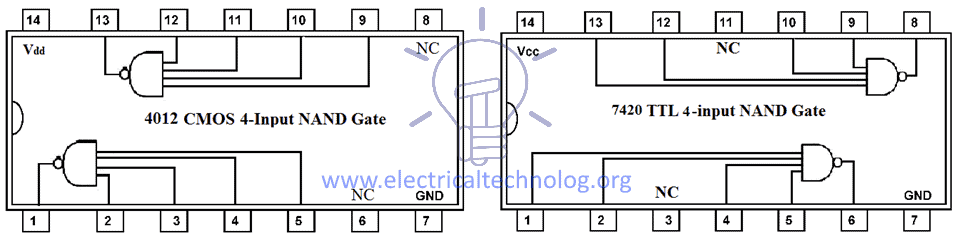
4012 CMOS and 7420 TTL NAND Gate IC (Four-Inputs)
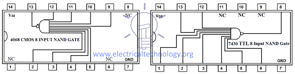
4068 CMOS and 7430 TTL NAND Gate IC (Eight-Inputs)
NAND Gate Applications
Logic NAND gate can be used in the following appliances and systems.
- Security Devices (Burglar or thief alarm system etc)
- Freezer warning buzzer
- Light activated systems
- Automatic watering system
- Safety thermostat configuration
- Push Button locks
- Storage devices like flash drive
- Cellphones, Computers, Calculators, LCD & Industrial controllers
You may also read more about Digital Logic gates
Logic NOT Gate – Digital Inverter Logic Gate
Digital Logic OR Gate
Digital Logic AND Gate
Exclusive-NOR (XNOR) Digital Logic Gate
Digital Logic NOR Gate