Ripple Carry And Carry Look Ahead Adder
Ripple Carry And Carry Look Ahead Adder – Logic & Block Diagrams
Ripple carry adder and carry look ahead adder are two different kinds of digital binary adders based on the carry determining technique.
Both adders can add the numbers without any problem. We will briefly discuss both adders in this article.
What is Ripple Carry Adder?
Ripple carry adder as the name suggest is an adder in which the carry bit ripple through all the stages of the adder.
The ripple carry adder contain individual single bit full adders which consist of 3 inputs (Augend, Addend and carry in) and 2 outputs (Sum, carry out). These full adders are connected together in cascade form to create a ripple carry adder. Fig 1. Ripple carry adder – Full Adder
‘n’ full adders combine together to form ‘n’ bit adder.
‘n’ bit adder will have ‘n’ stages and each stage’s output will depend upon previous stage’s carry out.
- You may also read: Counter and Types of Electronic Counters
Each stage can calculate the sum at the same time based on the input numbers but the sum will not be valid because the carry in to each of these stages will not be available yet.
For example in a 4-bit adder, there are 4 stages for each bit addition. The stage 1 being the LSB bit will first evaluate Sum, Cout and pass Cout to 2nd stage as Cin.
Then the 2nd stage will evaluate Cout and pass it to 3rd stage for calculation and then the 3rd stage will pass it forward to the 4th stage and now the 4th stage can evaluate the Sum and Cout. Now the sum we will get will be a valid output.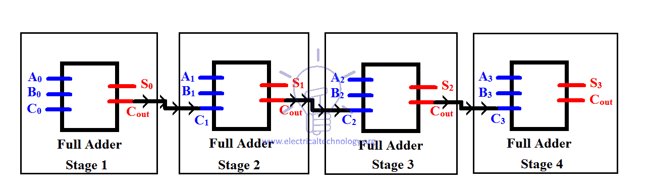 Fig 2 – Ripple carry adder Stages
In 4 bit adder, the time delay for a valid output is the sum of time delay of 4 full adders, if there is an ‘n’ bit adder, than the time delay will be the sum of time delay of ‘n’ full adders. It means, higher the bit size of the numbers, the late the answer we will get. So it is not an efficient design for complex and fast working systems.
The addition could be done as soon as the input numbers (Augend and addend) were provide to the adder but because of the carry propagation, the adder is not able to provide a valid answer until it reaches the last stage.
The time that the carry took to propagate from the first adder to the last adder is known as propagation delay. The major drawback of Ripple carry adder is this Propagation delay. But the design of Ripple carry adder is very simple and inexpensive.
- You may also read: What is ATMega Microcontrollers & How to Make an LED Project with it?
What is Carry Look Ahead Adder (CLA)
As we have discussed in the ripple carry adder that the adder takes a time delay to compute sum because the carry was propagated through all the gates from input to output. To increase the speed of the addition we need to provide the carry bits used by these adders without the wait for the preceding additions.
So that the addition of all bits is done at the same time.The idea used to compute the carry bits before the addition is known as Carry look ahead logic.
Carry look ahead is a digital circuit used for determining the carry bits used by the adder for addition without the wait for the carry propagation. It generates the carry bits for all the stages of the addition at the same time as soon as the input signal (Augend, addend, carry in) is provided.
Due to this technique the adders don’t have to wait for the carry propagation and a valid sum is computed without any delay.
- Also read: What is Raspberry Pi? Creating Projects using Raspberry Pi
Carry Look Ahead Adder (CLA) Logic Diagram
Carry look ahead adder’s (CLA) logic diagram is given below. It contains 3 blocks; “P and G generator”, “Carrylook ahead” block and “adder block”. Input “Augend”, “Addend” is provided to the “P and G generator” block whose output is connected with CLA and the adder block.
CLA block produces carry bits C1, C2, C3, C4 and provide it to the adder block and evaluate sum S0, S1, S2, S3, based on these inputs. C4 is taken as Cout.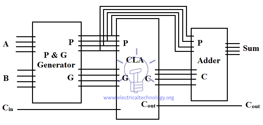 Fig 3- Carry look ahead Adder (CLA) logic diagram
- Also read: Automated Fingerprint Identification System and How it Works?
P and G Generator: Half Adder
This block consists of half adders used for generating P and G terms of each bit.
This block generate these terms needed for the CLA because the carry depends on it.
Carry = AB + Cin (A XOR B)
P = (A XOR B): P is known as Carry propagate, because it propagates the Cin from previous stage to the next stage.
G = AB: G is known as Carry Generate, because it can directly generate carry bit without any Cin.
P and G terms for a 4 bit number will be:
P0 = (A0 XOR B0) , G0 = A0B0 ,
P1 = (A1 XOR B1) , G1 = A1B1 ,
P2 = (A2 XOR B2) , G2 = A2B2 ,
P3 = (A3 XOR B3) , G3 = A3B3 ,
These P and G terms will be later used by CLA block.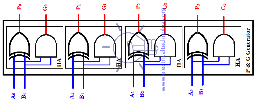 Fig 4- P and G Generator: Half Adder
Also read: Fully Automatic Water Level Controller using SRF04
Carry Lookahead (CLA) Block Diagram
CLA block contains combinational circuit used to determine the carry bits. it takes Augend, Addend and carry in as inputs and produce the carry bits.
Consider A, B two numbers being added both 4 bits wide and C0 as carry in. And C1, C2, C3, C4 are the output carry bits.
First we will derive C1,C2,C3,C4 using the carry equation from full adder.
Carry = AB + Cin (A XOR B)
P = (A XOR B)
G = AB ,
Carry = G + Cin P
So C1, C2, C3, C4 will become:
C1 = G0 + C0P0
C2 = G1 + C1P1 = G1 + (G0 + C0P0)P1 = G1 + G0 P1+ C0P0P1
C3 = G2 + C2P2 = G2 + (G1 + G0 P1+ C0P0P1)P2 = G2 + G1P2 + G0 P1P2+ C0P0P1P2
C4 = G3+ C3P3 = G3+ (G2 + G1P2 + G0 P1P2+ C0P0P1P2)P3 = G3+ G2 P3+ G1P2 P3+ G0 P1P2P3+ C0P0P1P2P3
Thus it shows that none of these carry bits depend on their previous stage carry bits. They only need A , B and C0.
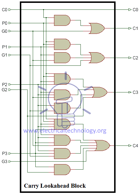 Fig 5 – Carry Lookahead (CLA) Block Diagram
This carry look ahead block will generate these carry bits and provide it to the adders block for addition.
- You may also read: Negative Feedback and Negative Feedback Amplifier Systems
Adders Block
As we know that the carry bits will be provided by the CLA block so we don’t need Full adders to evaluate the carry bits. We only need the sum which is:
S = CinXOR (A XOR B)
So the sum of each bit will be
S0 = C0 XOR (A0 XOR B0) = C0 XOR (P0)
S1 = C1 XOR (A1 XOR B1) = C1 XOR (P1)
S2 = C2 XOR (A2 XOR B2) = C2 XOR (P2)
S3 = C3 XOR (A3 XOR B3) = C3 XOR (P3)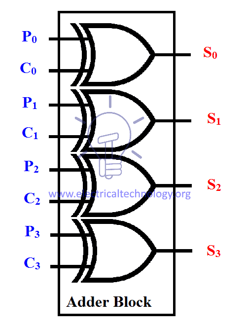 Fig 6 -Adder Block
And the last carry C4 will be the Cout of the CLA full adder.
Cout = C4
Full Schematic of Carry look ahead adder is given in figure below.
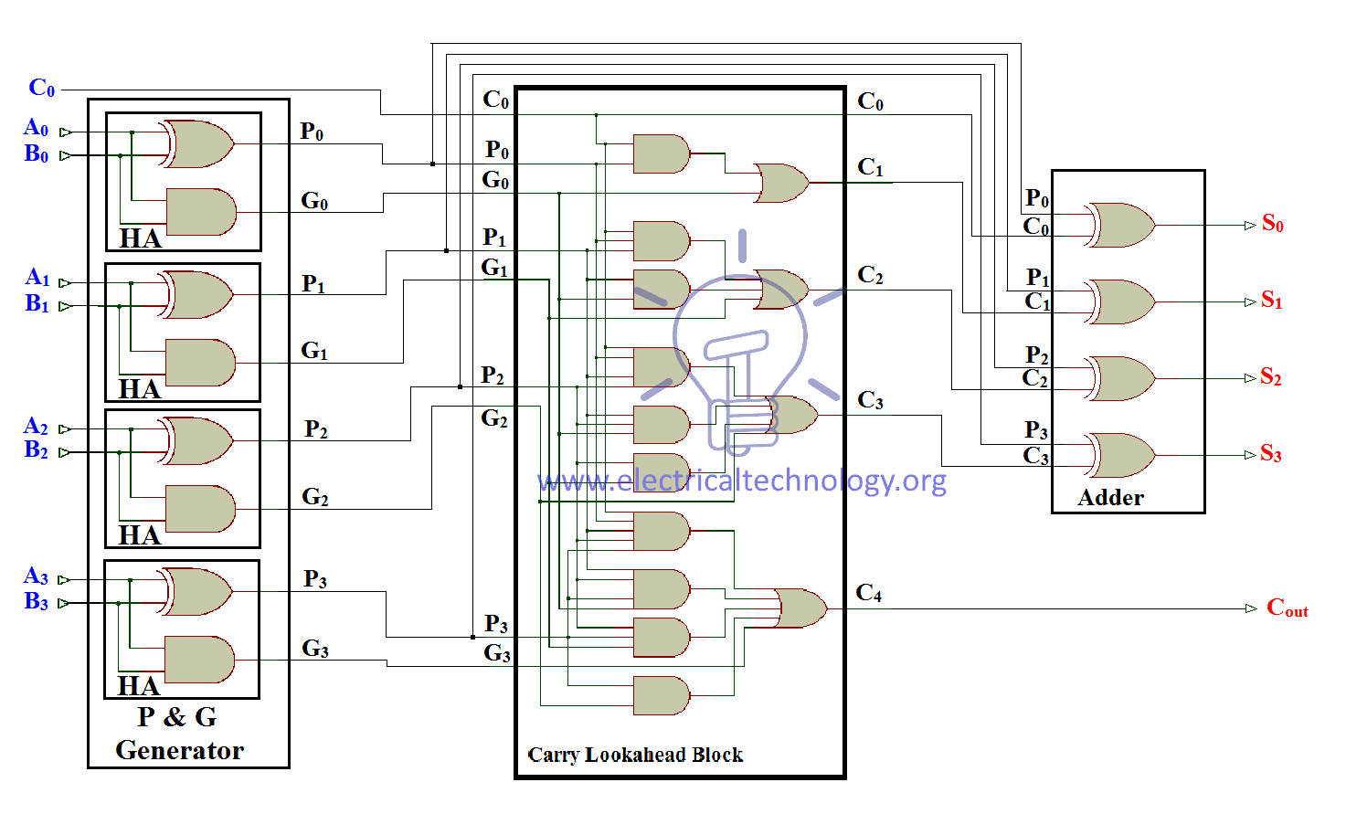 Fig 7 – Schematic Diagram of Carry look ahead adder
4-BIT Look-Ahead Carry Generator – 74182 TTL IC Details
74182 TTL is Carry generator working on Carry look ahead logic.
Inputs: P̅0 = invert of P0, G̅0 = invert of G0 Outputs: Cn= C0, G̅= COUT
P̅1= invert of P1, G̅1 = invert of G1 Cn+x= C1 , P̅=P̅0P̅1P̅2P̅3
P̅2= invert of P2 , G̅2 = invert of G2 Cn+y = C2
P̅3= invert of P3 ,G̅3 = invert of G3 Cn+z=C3
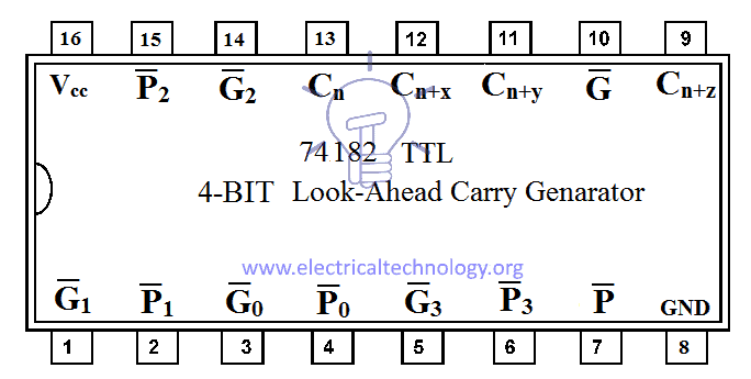 Fig 8: 4-BIT Look-Ahead Carry Generator – 74182 TTL IC Details
You may also read:
- 555 Timer
- What is Arduino and How to Program it?
- How To Design a PCB (Step by Step & Pictorial Views)