PCB Designing: How To Design a PCB – Example Circuit
PCB Designing: How To Design a PCB? – Example PCB Design of an LED Flasher Circuit
What is a PCB “Printed Circuit Board” ?
PCB stands for “Printed circuit board”. On this board all the components are soldered and interlinked by the copper tracks. The PCB can be a single layer and can go up to many layers as a person want, but most of the software support up to 14 layers.
Most commonly used PCB is a single sided PCB and the components and conductors on different layers of PCB are connected with plated-through holes called vias. PCB is designed in the software and then software file is given to the manufacturer and the rest of the work is all practical and not in the scope of this article. This article just covers how to design a PCB of a specific electronic circuit in software.
- Related Post: 25 Online PCB Design Tools and Software for EE Students

PCB Designing In Ares Capture Proteus.
Software Introduction:
Software which we are going to use in this tutorial is Labcenter electronics release most commonly known as ARES PCB. This is fully professional software. its student version is also available to download free but with limited functionality.
This software support up to 14 layers of PCB and it is highly equipped with all the modern tools which able to make an effective and accurate PCB. We can change the width of tracks, pads according to the application. Designers can design the custom board shape. The Output of this software can have different format selectable by the designer e.g. PCB can be exported in PDF, JPEG and lots of other formats.
Its library includes thousands of commonly and rarely uses through hole and SMD devices. There is also a category for miscellaneous parts. There is one more very useful tool available by which we can make footprints of all the devices whom footprints are not available in the library so we can say that this software covers all the needs of the PCB designer and strongly recommended by the professionals.
Step by Step PCB Designing Tutorial: (in our example, we will use the LED Flasher Circuit and design its PCB).
Note: it is considered that you have installed the software and have basic knowledge of electronics.
Step1.
Click on this icon to run the software.![]()
If you installed this software correctly then this window will appear on the screen.
This black screen is the work place. All your PCB work will come here and the blue dot which appear in the center of the black gridded screen is the center of the work place.
Step 2.
Make a list of the components and devices according to your schematic / electronic circuit.
Note: it is considered that you have already drawn an error free schematic diagram of the circuit and you want to make the PCB Design of that schematic circuit.
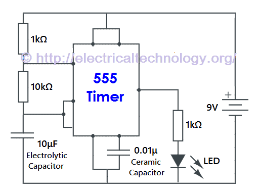
In this simple example of PCB designing, we are using the below schematic. This is the basic Electronics LED flasher circuit with one LED by using 555 Timer and other basic electronic components.( Detail of the parts can be found in Step 3 ).
Step 3.
Now we have to find the parts. As you can see we need the following basic electronic components for LED Flasher Circuit where flasher means continuously ON & OFF.
- 1) The base for 8 pin 555 Timer IC.
- 3 Resistor of ¼ watt rating ( two are 1kΩ and last one is 10kΩ).
- 2 axial capacitor (one is 10μF electrolytic and second one is 0.01μF ceramic Capacitor).
- 5 MM LED (Red Color).
- Power connector.
- 9V DC Battery.
Each of these parts can be searched by the category in which they fall.
Step 4.
Now click on this button on the left side vertical bar. When you scroll over it shows package mode.
And when you click on the package mode on the white area you will see two buttons on which “P” and “L” is written.
Step 5.
Now Click on “P”. When you click on “P”, New window will appear and on that window you will find all the part.
As you can see there are categories and types. Selected the desired category and then select the appropriate type and all the components matching the above criteria is will show up in the white space as shown in the above window.
Suppose, we want to search for the resistor of ¼ watt. We search that part like this.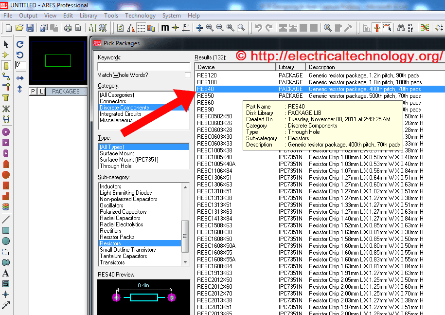
Step 6.
Select “RES40” because it is ¼ watt resistor.
Double click on that RES40 package and this package will be added to the left side vertical white space where Packages is written on the design window.
Like this one.
Now in the same way search of capacitor in the “type” menu and choose “CAP20”.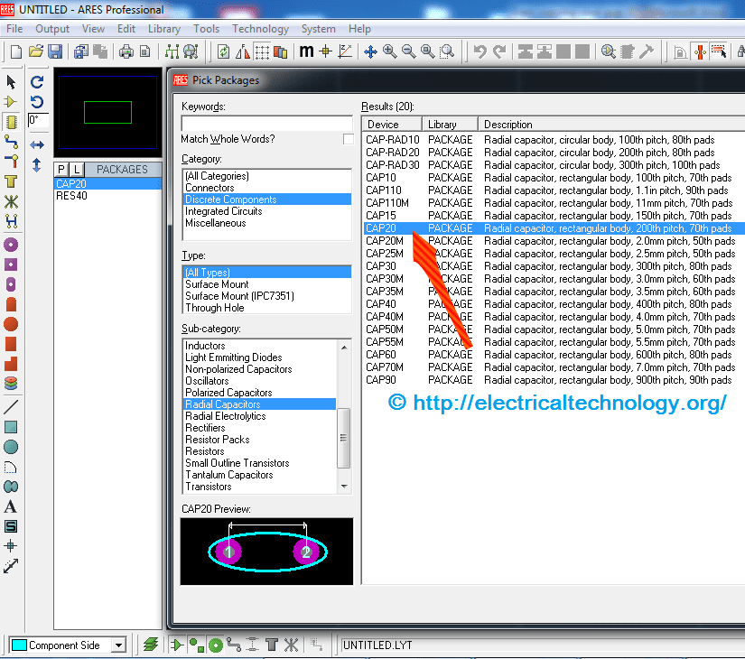
Now we need 8 pin DIL (Dual in line package) for 555. Search it like the previous components.
Now last thing you need is the power connector to connect the wires to the board.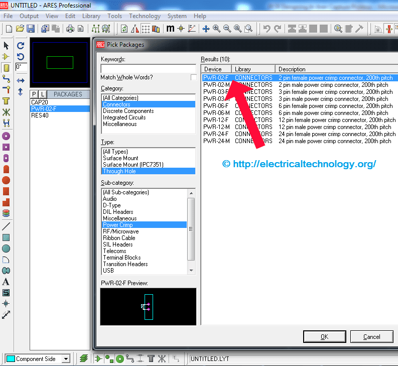
Step 7.
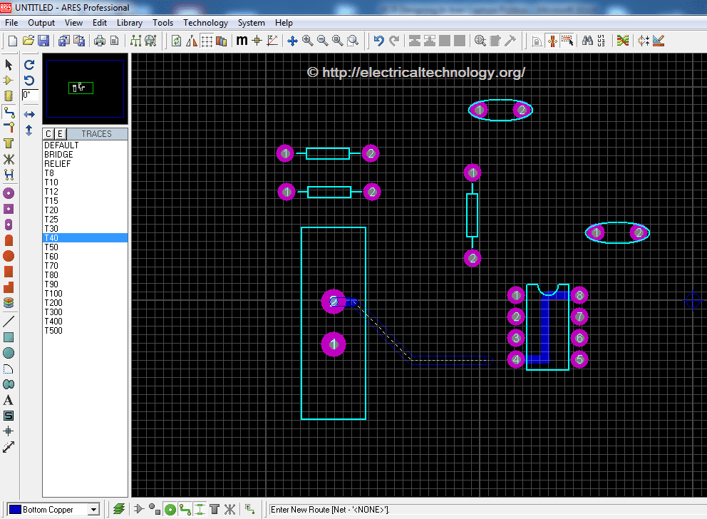
Once all the components are added now you can start routing the PCB.
Put all the desired components on the workplace like this.
Step 8.
Now you have to connect them according to the schematic.
For connecting all the components, you have to use the wire tool which is available on the left side of the window in the vertical bar.
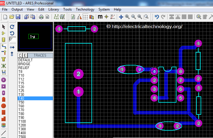
Step 9.
After selecting the track mode, now you can start routing. As you can see the default pads are very narrow you have to choose the appropriate pads for the components whom pads are narrow.
Choose pad Mode (As shown below).
Step 10.
After that, put the appropriate pad on all the narrow pad and then start routing.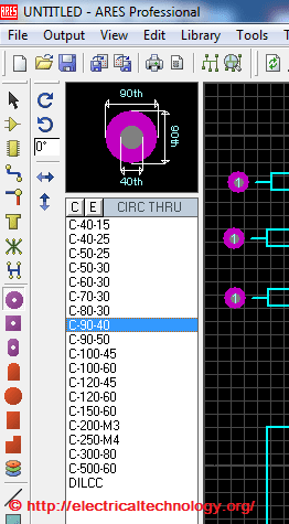
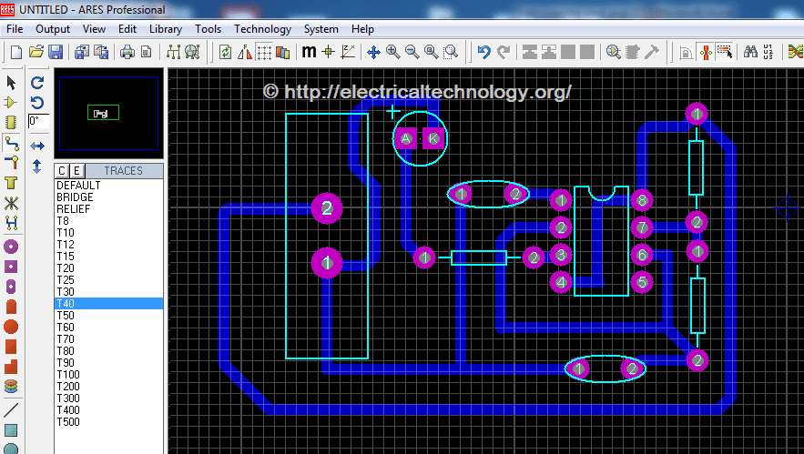
Step 11.
Connect the components according to the schematic.
In process …
Completed PCB Design of LED Flasher Circuit.
Step 12.
Now select the “board Edge” layer form the left bottom layer selecting Drop down menu.
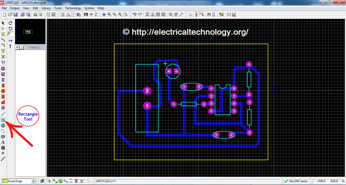
Step 13.
After selecting the board edge layer, draw a rectangle around your PCB art work. This will be your PCB Board dimensions.
Select the rectangle from the left side menu.
This is all about the basic and simple PCB designing, more technical details will be posted in the further post. Stay tuned.
Also, Don’t forget to subscribe. Simply, Enter your email address and hit enter in the below box and we will notify you by email for other tutorials like this one. :) Thanks.
Related Posts:
- How to Program PIC18 Microcontroller. Step by Step Tutorial.
- Arduino Programming: What is Arduino and How to Program it?
- MAX232: Construction, Operation, Types and Application.
- 10+ Design & Simulation Tools for Electrical/Electronics Engineers Online.
- 15 Must Have Android Apps for Electrical & Electronics Engineers & Students.
- Top & Best Books & Guides for Electricians and Apprentices
- Clap Switch Circuit Electronic Project Using 555 Timer.


thanks for help
Dear admin i want every new and old sort of question papers for the electricity board exams and the books and concepts of electrical and electronics engineering.
There’s a mistake in your final design. 555 Pin 1 is supposed to be grounded(555 GND pin), while pin 5 (555 CV pin) goes to ground via capacitor.
Nice sir, I am only beginner.