555 Timer IC- Types, Construction, Working & Application – Circuit & Pinout
555 Timer IC – Mode of Operation – Schematic, Internal, Block Diagram & Applications
Digital Timers
Timers are those circuits, which provide periodic signals to a digital system which change the state of that system. In other words, those circuits, which work on the base of multivibrator changes or a device, which can be used as multivibrator is called Timer. The 555 Timer IC is one of them, and we will discuss it in detail in the following article.
What is 555 Timer IC?
555 Timer is a digital monolithic integrated circuit (IC) which may be used as a clock generator. In other words, 555 Timer is a circuit which may be connected as a stable or monostable multivibrator. In more simple words, 555 Timer is a monolithic timing circuit, which can produce accurate timing pulses with 50% or 100% duty cycle. It was developed in the year 1970 by Signetic Corporation and designed by Hans Camenzind in 1971.
555 Timer is a versatile and most usable device in the electronics circuits and designs which work for both stable and monostable states. It may provide time delay from microseconds up to many hours.
555 timer is a very cheap IC which works for wide range of potential difference (typically, from 4.5 to 15V DC) and the different provided input voltages do not affect the timer output.
555 Timer is a linear device and it can be directly connected to the CMOS or TTL (Transistor – Transistor Logic) digital circuits due to its compatibility but, interfacing is must to use 555 timer with other digital circuits.
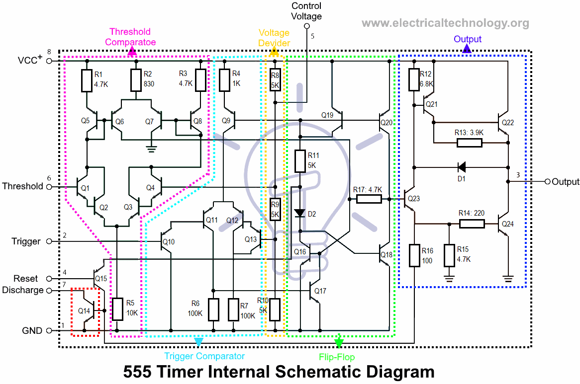
Being an integral part of electronics project, 555 Timer IC is very often used in simple to complex electronics projects. The standard 555 timer IC is made of 2 diodes, 25 transistors, 15 resistors installed in an 8 pin dual in-line package.
This timer is called 555 Timer due to the fact that it contains three 5 Kilo-Ohm resistors in series to form the voltage divider pattern.
Related Post:
- Binary Encoder – Construction, Types & Applications
- Binary Decoder – Construction, Types & Applications
Features of 555 Timer IC
- There are two types of 555 timer based on its nomenclature – NE 555 Timer and SE 555 Timer. While NE 555 timer can be used in the temperature range from 0 to 70°C, the SE 555 Timer can be used in the temperature range from -55°C to 125°C and has a temperature stability of 0.005% per 0C..
- it can be operated of different power supplies ranging from 5 Volts to 18 Volts.
- It can be used either as a pulse generator or an oscillator by operating it in different modes.
- The name 555 comes from the fact that it contains three 5 Kilo-Ohm resistors in series to form the voltage divider pattern.
- It can drive both Transistor-Transistor Logic (TTL) due to its high output current and CMOS logic circuits.
- It has high output current and adjustable duty cycle.
- 555 timer can be operated in both astable and monostable modes.
- The output of 555 timer can source or absorb current up to 200mA sinking or sourcing current to the load.
- It contains 24 transistors, 2 diodes and 17 resistors.
- 555 timer is available as an 8-Pin Dual in Line Package (DIP), 8-Pin Metal Can or 14-Pin Dual in Line Package (DIP).
Related Articles:
- Digital Asynchronous Counter (Ripple Counter) – Types, Working & Application
- Digital Synchronous Counter – Types, Working & Applications
555 Timer Construction & Block Diagram
There are lots of manufacturers who manufacture 555 timer which included the number 555 e.g. NE555, CA555, SE555, MC14 555 etc. typically, two 555 timers sandwiched inside a single chip which is called 556. Nowadays, chips are available with four 555 timers in it. These devices are available in circular IC with eight (8), DIP (Dual inline Package) with 8 pins or DIP with 14 pins.
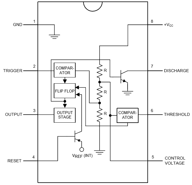
Below is the pin diagram of DIP (Dual inline Package) 555 timer with 8 pins.
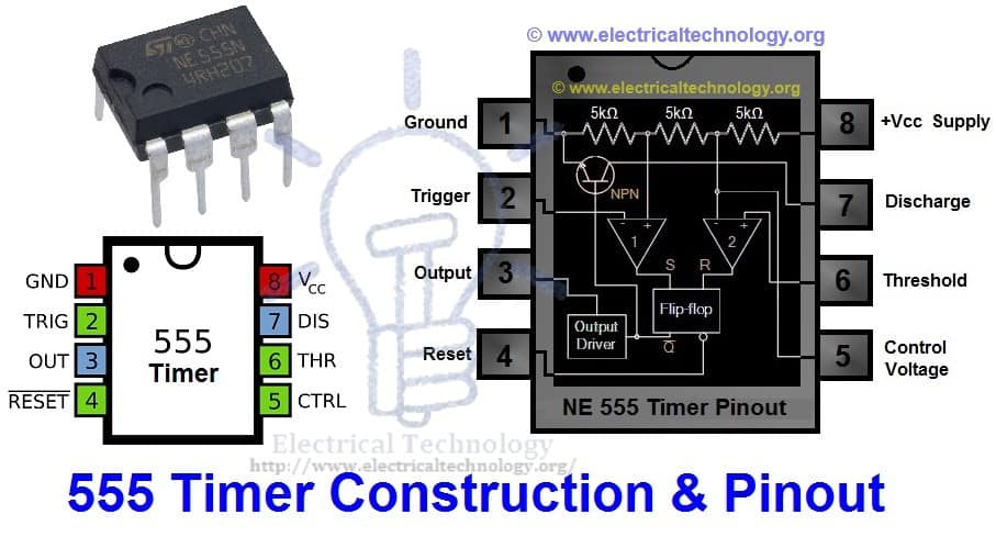
A simple 555 timer circuit is shown above in fig 3 which shows the internal construction of 555 timer. According to fig 1 & 3, the timer contains on two comparators, an RS flip flop, an Output stitch (output buffer) and a Discharge Transistor Q1.
In addition, there are three 5kΩ resistors are connected in series with 5kΩ resistor which first end is connected with VCC (Pin 8 = Supply voltage) and the other end is connected with ground (GND = Pin 1).
In above fig 1 and (as well as below fig 2 & 3), As given in the block diagram, heart of the IC lies in the two comparator circuits. While inverting terminal of the upper comparator is connected to a point with DC potential of 2/3 VCC (where VCC can be +5V to +18V), the non-inverting terminal is connected to the threshold pin.
The inverting terminal of the lower comparator is connected to the external trigger input pin whereas the non-inverting terminal is connected to the point with DC potential of 1/3 VCC. The three 5 Kilo-Ohm resistors are connected in series to form voltage divider circuit. Output from both the comparators is given to the R-S Flip Flop whose state depends on the output from the two comparators.
Output from the R-S Flip-Flop is connected to the two transistors – Q1 and Q2. Q1 is the discharge transistor and provides discharge path to the external capacitor, when saturated. Q2 is the reset transistor, where a pulse applied will reset the whole timing circuit. The output from the flip-flop is amplified by the power amplifier block.
Related Articles:
- MUX – Digital Multiplexer | Types, Construction & Applications
- DEMUX – Demultiplexer | Types, Construction & Applications
555 Timer Pinout Configuration
| 555 Timer IC Pinout | ||
| PIN Number | Name | Purpose |
| 1 | GND | Ground reference(0V) |
| 2 | TRIG | To give external trigger voltage |
| 3 | OUT | 1.7V below +VCC or to GND |
| 4 | RESET | To reset timing interval |
| 5 | CTRL | Provides control access to internal voltage divider |
| 6 | THR | Threshold voltage |
| 7 | DIS | In phase with output |
| 8 | VCC | Positive voltage supply |
Here is the simple explanation of the 8 pins of 555 Timer IC (Fig 1 & 2). Let’s understand this IC with its pin configuration and circuit diagram.
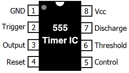
1. Ground (GND)
It’s the common ground point of the circuit. The ground terminal of external circuit as well as power supply (VCC) ground terminal is connected to the GND (Ground) terminal of 555 timer.
This pin is either grounded or connected to the negative rail. Connection using a resistor is not recommended to avoid heating up of the IC because of the stray voltage accumulated inside it.
2. Trigger
When Trigger terminal gets one –third (1/3) of the supply voltage i.e. VCC/3 equal amplitude’s negative trigger pulse, then the circuit output changes form Low to High.
This pin is the input trigger pin to the IC and activates the timing cycle. A low signal at this pin triggers the Timer. Required current at this pin is 0.5 uA for a period of 0.1 uS. To avoid false triggering due to noise, the pin requires a pull up connection. Voltage at this pin is 1.67 Volts for a supply voltage of 5 Volts and 5 Volts for a supply voltage of 15 Volts.
3. Output
This terminal is used for getting output and connected with load. At any instant, its value is low or high. i.e. This is the output pin of the Timer. Output of the Timer depends on the duration of timing cycle of the input pulse. The output can either sink or source current, at maximum 200mA.For LOW output, it sinks current, voltage being slightly greater than zero and for HIGH output, it sources current, voltage being less than VCC.
4. Reset
Without taking into account the previous state of output, by providing a trigger pulse to this terminal resets the device. I.e. Its output becomes low.
The reset pin is either not connected or connected to the positive rail. A logic LOW signal at this pin resets the Timer regardless of its input. The required reset voltage is 0.7 Volts, at current of 0.1mA
5. Control Voltage
There are two third positive voltages of the total Supply voltages (VCC) at control voltage terminal. Thus, it becomes a part of the comparator circuit. Generally, a capacitor is connected between ground and voltage control terminals.
This is also a generally non-connected pin or connected to ground through a 0.01uF capacitor. For some applications, this pin is required to control the threshold voltage at the upper comparator and is connected to an external DC signal, to change the duty cycle.
6. Threshold Voltage
Threshold voltage and control voltage is the two inputs of comparator circuit. The circuit compares the available voltage at threshold voltage terminal to the available reference voltage at control terminal.
If the available voltage at threshold terminal (Pin 6) is greater than the control voltage i.e. two-third of VCC, then the output would be low, otherwise, it would be high.
This pin provides threshold voltage to the upper comparator. When voltage at this pin is greater than 2/3 VCC, the duty cycle is changed. It is connected to non-inverting terminal of the upper comparator. Required current is 0.1 mA, with pulse duration of 0.1 uS.
7. Discharge
When output is low, then Discharge terminal provides a low resistance discharge path to the externally connected capacitor. However, it acts an open circuit, when output is high.
This pin provides a discharge path for the timing capacitor through the NPN transistor. A discharge current less than 50 mA is required to avoid damage. It can also be used as open collector output.
8. +VCC (Supply Voltage Terminal)
Supply voltage is provided at this terminal for timer operation. This pin is connected to positive rail of the Power supply and is also known as VCC. The supply voltage can vary from +5 Volts to +18 Volts.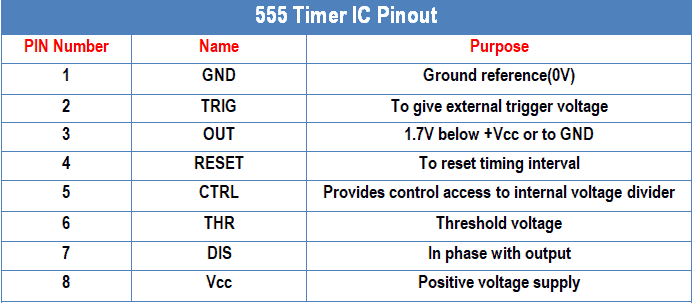
Related Posts:
Schematic & Working Principle of 555 Timer IC
In the 555 Timer block or functional diagram, comparators are those devices which output is high, when their positive input voltage is greater than their negative input voltage and vise versa.
Internal Function Diagram of 555 Timer
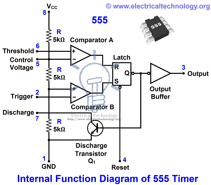
The voltage divider in the circuit (which contains on three series connected 5kΩ resistors), which provides the trigger level of one-third of VCC (VCC/3) and two-third (2/3) of threshold voltage. To understand this point, suppose the input value is 15V. In this case, the value of trigger level would be 5V as (VCC/3 = 15V/3 = 5V). And the value of threshold level would be 10V as (VCC x 2/3 = 15V x (2/3)) = 10V.
When needed, the trigger level and threshold can be adjusted by using the Control Voltage terminal (Pin 5) i.e. by changing the control voltage at Pin 5, we may change the trigger level and threshold voltage according to the required specification. However, in this case, the value of trigger and threshold would be remain equal to 1/3 VCC and 2/3 VCC respectively.
Coming to the working part of 555 Timer IC, this circuit generally operates in three different modes namely A-stable, Mono-stable and Bi-stable modes. For a better understanding of 555 Timer IC and its different states, check the below circuit diagram.
- Related Post: Counter and Types of Electronic Counters
555 Timer Internal Schematic Diagram
When the normal high trigger input value instantaneously reduce then the 1/3 VCC, Then the output of Comparator B becomes High from Low, as a result, RS latch or RS Flip flop goes to “set”. When flip flop goes to set, then Output (at Point 3) becomes high. Simultaneously, the discharge transistor Q1 gets off and The output remains high until the value of normally low threshold input does not increase then the 2/3 VCC.
As soon as the threshold input increase than the 2/3VCC, then the output of comparator A becomes Low, as a result, RS flip flop get reset (because the output of comparator is directly connected to the RS flip flop’s input R as shown in the fig). When flip flop gets reset, output becomes low and discharge transistor Q1 goes to on.
The flip flop can be reset by applying external input reset without threshold circuit. Note that, the trigger and threshold inputs (Pin 2 and Pin 6) are controlled by externally components and the 555 timer can be used as stable , monostable or bi-stable operation by controlling the trigger and threshold inputs with the help of those external components.
- Related Post: Digital Logic AND Gate
Types of 555 Timers & Operating Modes
There are three basic types of 555 Timer with respect to mode of function and operation.
- 555 Timer as Astable Multivibrator
- 555 Timer as Monostable Multivibrator
- 555 Timer as Bi-Stable Mode
555 Timer can be operated in three modes – Monostable Mode, Bi-Stable Mode and Astable Mode.
Astable Mode:
In this mode, there will be no stable level at the output and the output will keep swinging between high and low. i.e.- It doesn’t have any stable state and keeps switching between high and low without application of any external trigger.
Working of 555 timer in A-stable Mode
The trigger and threshold pin are connected together so, there is no need of external trigger pulse. The comparator will output 1 while charging the trigger because the input voltage at trigger pin is still lower than 1/3 of supplied voltage.
This time, the output of timer is high. Once the voltage across reaches 1/3 of the supplied voltage, the trigger comparator will output 0,keeping the situation unchanged as both R and S input of flip flop are 0.Once the voltage across the capacitor reaches 3/7 of applied voltage, the threshold comparator will output 1 to R input of the flip-flop.
Now, the capacitor will start discharging through resistor R2 and discharging transistor. The output of 555 Timer is low at this point. Once the voltage across capacitor drops to 1/3 of the supplied voltage, the trigger comparator will output 1.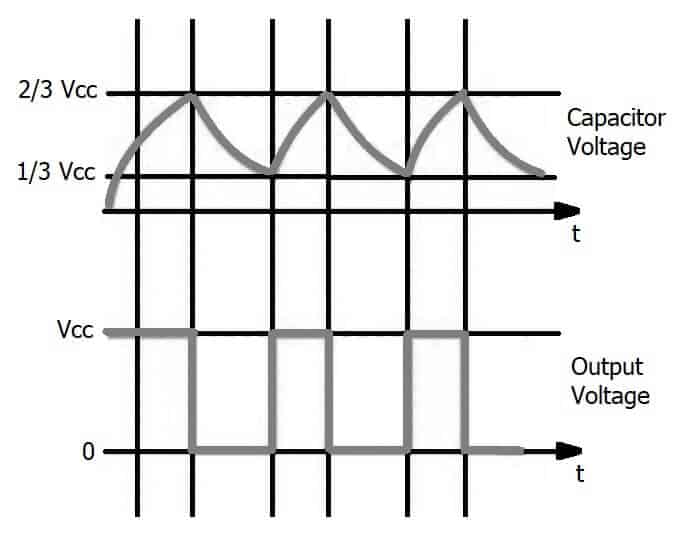
You can easily calculate the output of this configuration using the below mentioned formula. The high time depend on resistors R1, R2 and capacitor. On the other hand, low time depends only on resistor R2 and capacitor.
High Time:
TH = 0.693 x (R1 x R2) XC1
Low Time:
TL = 0.693 x (R2) X (C1)
Period for one cycle:
T = TH +TL x (R1+ 2R2) C1
Frequency:
f =1.44 / (R1 + R2) C1) HZ
It is also known as self-triggering mode, the Timer is used in this mode as clock pulse generator or oscillator. The Timer switches between two quasi stable states and without any external trigger input.
Given below is 555 Timer circuit in Astable mode.
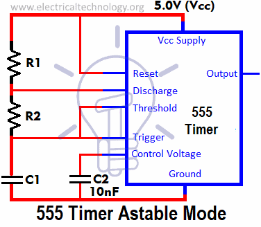
(Ref Fig 2 as well) As the Timer is switched ON, i.e. the output is HIGH, the transistor Q2 will be in cut off region on receiving a LOW input signal. The capacitor charges through both the resistors R1 and R2 toward VCC. The capacitor charging time being
τ1 = 0.693 (R1 + R2)*C.
This capacitor voltage is the threshold voltage to the upper comparator.
As the voltage exceeds 2/3 VCC, the upper comparator output resets the Flip-Flop, which turns the Timer output to OFF state (provided reset pin is in LOW state) The transistor τ will in saturation region, i.e. will be turned ON, providing a discharge path for the capacitor through resistor R2, the discharge time being – 0.693 R2*C.
As the capacitor voltage falls below -1/3VCC, the second comparator output sets the Flip-Flop, which makes the Timer output LOW and the whole process starts again. Thus the Timer output oscillates between HIGH and LOW state, generating oscillations.
You may also read:
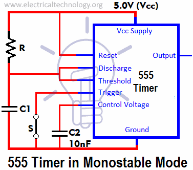
Monostable Mode:
This configuration consists of one stable and unstable state. If the stable output is set at high then the output of timer is high.
Working Of 555 Timer In Mono-Stable Mode
The trigger input is held high by connecting it to VCC through resistor. Threshold pin is low making the threshold comparator out 0. IN result, voltage coming from source is going to ground through the transistor. Press the pushbutton on trigger to change the 555 timer output to high.
At the same time, capacitor C1 will start charging through resistor R1. The 555 timer will remain in this position until the voltage across capacitor reaches 2/3 of the supplied voltage. Comparator will output 1 to R input of the flip flop bringing the circuit into initial state. The amount of time the timer output will remain high; depend entirely on value of both the capacitor C1 and resistor R1.
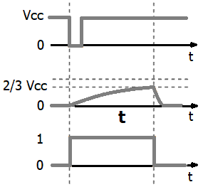
To calculate the time, use the below formula:
T = 1.1 * C1 * R1
It is also known as single shot mode or pulse generating mode. In this state, the 555 Timer is normally in a stable state until triggered, after which it jumps to the quasi stable state.
Given below is 555 Timer circuit in a monostable mode.
(Ref Fig 2 as well). Initially the Timer output is LOW and the transistor Q2 is in saturation mode, i.e. Fully ON. As a negative trigger pulse, more negative than -1/3 VCC, is applied to the second comparator, the Flip Flop sets to HIGH, turning the Timer output to HIGH state and the Transistor τ is turned OFF.
The output remains HIGH for time Tou i.e τ = 1.1 RC, i.e. the time taken for Capacitor C to charge (Also known as Time Constant RC). As Capacitor voltage exceeds 2/3 VCC, output from the upper comparator resets the Flip-Flop to zero and the discharge transistor Q2 gets again saturated, providing a discharge path to the capacitor. As the capacitor voltage comes back to zero volts, the circuit comes back to its normal state.
- Related Post: Two-Level Logic Implementation
Bi-Stable Mode:
In this configuration, both the output states are stable. At each interrupt, the output changes from low to high and vice-versa If we have a high output, it will go low once it receives an interrupt and stays low until the next interrupts changes the status.
Working of 555 Timer in Bi-stable mode:
The Trigger and the Reset pins of the 555 Timer IC are connected to VCC through the two resistors. To keep the input state low while holding them pushed, connect the two pushbuttons between these pins and ground.
After pressing the trigger button, the trigger input state will become low. Consequently the comparator will output High and that will make flip-flip Q-bar output go Low. The final state of the timer state will be high .The output will remain high even when the trigger pushbutton is not pushed because in that case the R and S input of flip-flop will be 0 which means that the flip-flop won’t change the initial state. To make the output low, we need to reset the pushbutton which eventually Resets the entire 555 Timer IC.
This is also known as Flip-Flop mode and the Timer remains in two stable states in this mode. It does not require any external timing circuit as the time delay between two states depends upon the timing of application of external pulses.
- Related Project: PCB Design of LED Flasher Circuit using 555 Timer. Step by Step
Given below is 555 Timer circuit in Bi-Stable mode.
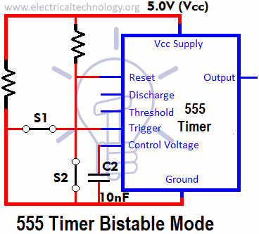
Two switches are connected as such that while Switch S1 is connected to reset pin with VCC, switch S2 is connected to trigger pin with ground. A negative going pulse, at the trigger input, at voltage more negative than -1/3VCC, triggers the lower comparator output to set the Flip-Flop and thus the Timer output to be HIGH. As the threshold pin is grounded, a positive going pulse at the reset pin triggers the
Since the Timer remains in one stable state until an external pulse is applied and then changes to another stable state, this mode is termed as Bi-stable mode. An important application is the Schmitt Trigger circuit.
555 Timer Calculator
The calculator can see under the title “555 Timer Calculator with formula & Equations“
Applications of 555 Timer
555 timer is most important integrated circuit (chip) used widely in digital electronics. Some common uses and application of 555 timer IC are as follow:
- PWM (Pulse Width Modulation) & PPM (Pulse Position Modulation)
- Duty Cycle Oscillator
- Lamp Dimmer
- To provide Accurate time delays
- As a flip-flop element
- Digital logic probes
- Analog frequency meters
- Quad Timer applications
- Pulse, Waveform, and square wave generation
- Stepped tone & tone burst generator & linear ramp generation
- Tachometers & temperature measurement
- It can be used as monostable multivibrator and astable multivibrator
- DC to DC Converters
- DC Voltage Regulators
- Voltage to Frequency Converter
- Frequency Divider
- Schmitt trigger
- Cable tester
- Pulse detector
- Wiper speed control
- Timer Switch
- Time delay generation, precision timing and sequential timing
- The 555 Timer IC are widely used in most of interesting electronic circuits and project like Traffic Light Circuit using 555 Timer, LED Flashing circuits, police siren, LED dice, Music Box, Metal detector, Joystick and game paddles, & low cost line receiver, Clap switch activated circuit and lots of other projects and circuits designs.
This is the basic tutorial about 555 Timer IC. Any other information regarding 555 Timer is welcome in the comments section. We hope that you have got a better understanding of 555 Timer IC and its working in different configurations.
Related Posts:
- Thyristor – Silicon Controlled Rectifier (SCR)
- Microcontroller – Types of Microcontrollers & their Applications
- Microprocessor – Types of Microprocessors & their Applications
- How to Program PIC18 Microcontroller in C
- MAX232: Construction, Operation, Types and Application
- PCB Design of LED Flasher Circuit using 555 timer (How To Design a PCB)?
- What is Negative Feedback and Negative Feedback Amplifier Systems
Basic Electronic Projects circuits based on 555 Timer
- Basic Voltage Doubler Circuit Diagram using 555 Timer IC
- LED Roulette Circuit Diagram using 555 Timer & 4017 Counter
- Simple Touch Sensitive Switch Circuit using 555 Timer & BC547 Transistor
- Clap Switch Circuit Using IC 555 Timer & Without Timer
- Traffic Light Control Electronic Project using IC 4017 & 555 Timer


that is great.how can singleph,twophase and threephase changeover be fix.
i want to information of generated electrical energy by piezoelectrical tansducer
Marvelous, what a blog it is! This web site presents valuable facts
to us, keep it up.
where i found circuit of traic ???? ohhhh i for get to say thankkkkkkkkkkkkkkkkks a lot
Hi Ahmad,
You can see the full article with circuit diagram on TRIAC here.
It appears that the pin diagram for the 555 chip is incorrect.
Your pinout of the555 is wrong. the pins 1-8 run around the chip anticlockwise.
Thank you for your correction. It has been modified now.
Nice work
Pinout numbers are incorrect for Fig 2, they are correct for other pics.
nice web page – thanks!
Thank you for correction. It has been modified now.
Fig. 3. Q21 is NPN. Drawing shows wrong PNP. This way it would short the supply directly to ground and burn down Q22 and Q24.
Fig.5. is not symmetric oscillator.
For less part count and guaranteed precise equal 50% duty cycle see
https://bit.ly/3FsOFkZ regardles the RC factor determining the frequency.
Note that load cannot exceed 200mA otherwise it needs external transistor.
Haw many voltage is the construction take?