What is PNP Transistor? Construction, Working & Applications
PNP Transistor – BJT Transistor Construction, Working & Applications as Switch & Amplifier
Transistors are smaller than vacuum tubes, and were invented by J. Barden and W.H. Brattain of Bell Laboratories, USA. When a third doped element is added to a diode in such a way that two-PN-junctions are formed, the resulting device is called a transistor.
What is PNP Transistor?
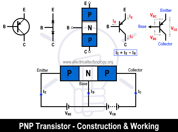
The construction of a PNP transistor is done as the name suggests by taking an N-type semiconductor material and sandwiching that in between two P-type semiconductor materials. In reality, the P-type material is generally a lot thicker in width compared to the N-type material.
The emitter of the PNP transistor is highly doped and the base of it is lightly doped while the collector is moderately doped. When differentiating the layers of a transistor according to the area they take in the device, base is very thin, collector is large because it has to dissipate heat, and emitter is moderate in thickness.
A transistor has two PN-junctions of which one is forward biased while the other is reversed biased. The path for the carriers through the forward bias has low resistance and through the reverse bias has high resistance. A weak signal is fed as input at the low resistance circuit and output is taken from the high input circuit.
Therefore, a transistor transfers a signal form low resistance to high resistance. It transfers the resistance from one circuit to another, hence named as transistor. It’s made from the words transfer and resistor. The majority carriers in these types of transistors are holes and the minority carriers are the electrons.
Construction of PNP Transistor
A transistor has three sections of doped semiconductors. It has emitter on one side and the collector on another. The middle portion is called the base. Below we have described all the three parts of the transistor.
Emitter:
The work of the emitter is to supplies charge carriers. To supply a large number of charge carriers, the emitter is always in forward biased when compared to the base.
Base:
The middle section of the transistor, which forms the two PN-junctions between emitter and collector, is called the base. The base-emitter junction is forward biased allowing a low resistance for the emitter circuit. The base-collector junction is reverse biased which provides a high resistance in the collector circuit.
Collector:
The section on the other side of the emitter that collects the charges is called the collector. The collector is always reverse biased.
Because the transistor has two PN-junctions, it is like two diodes. The junction between the emitter and base may be called emitter-base diode or emitter diode. Similarly, the junction between the collector and base can be called collector-base diode or collector diode.
From the configurations of the PN junctions as given above, we can make out that the emitter diode is always forward biased and the collector diode is reverse biased. The PNP transistor is a current-controlled device.
The PNP transistor configuration is shown below.
The above diagram shows the schematic diagram of the PNP transistor, though the thickness of each layer is not to scale. The symbolic representation of the PNP transistor is the same as that of another type of transistor NPN except that now the direction of the arrow is from emitter to base whereas in NPN transistor, the arrow points from base to emitter.
Voltage across the base and emitter is according to the junction bias. This makes the base negative and the emitter positive. The base is always negative biased with respect to the emitter. As collector voltage is always less than the base voltage and the base voltage is less than the emitter voltage, generally in a PNP transistor, the emitter voltage is always more positive than the other two terminals.
The two transistors PNP and NPN can be used interchangeably in most electronic circuits, taking into account the polarities of the voltages and the current flow’s direction.
Given that there are two types of transistors, there can be a difficulty in identifying a given transistor for proper usage. To properly identify a device, we need to have a proper understanding of the device with which we are working with. As we have already discussed, the PNP transistor is a device made of two diodes connected end to end.
We can use our knowledge of diodes to identify the type of transistor we are working with. Also along with the unidirectional conducting properly of diodes, we can also make use of the different resistance that the transistor offers across different terminals in a way to confirm our prediction of the device. To identify the device, the following points are to be kept in mind,
Emitter-Base terminal: There is a diode in between the emitter-base terminals so those two terminals should function as a normal diode and conduct in only one direction.
Collector-Base terminal: There is a diode similar to the collector-base terminals. These terminals again should act as the terminals of a normal diode, and conduct only in one direction.
Emitter-Collector terminals: The Emitter-Collector terminals are not connected internally and hence will not conduct in either direction.
The table below shows the terminal resistance values for PNP transistors.
| Between Transistor Terminals | Resistor Values | |
| Collector | Emitter | R_high |
| Collector | Base | R_low |
| Emitter | Collector | R_high |
| Emitter | Base | R_low |
| Base | Collector | R_high |
| Base | Emitter | R_high |
We can say that a PNP transistor is normally in NO (Normally Open) state. For the transistor to start conducting, we need to conduct a small output current and apply a comparatively more negative voltage at the base terminal relative to the Emitter terminal.
In short, the PNP type of transistor will conduct when voltage at emitter is much greater than the voltage at collector. When in ON state, the current flow through Emitter-collector is much higher than the OFF state.
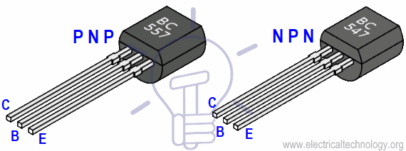
The following fig shows the BC547 NPN and BC557 PNP transistor.
Biasing & Working of a PNP Transistor
As discussed above, the PNP transistor can be said to be naturally in Normally Open state. Switching ON the PNP transistor requires us to make the voltage at the base terminal lower than that of the emitter terminal.
When turned ON, the current that is generated from the majority carriers, in this case the holes, starts flowing from the base-emitter part of the transistor. This flow of current then flows to the base and then finally to the collector.

From the direction of the current flow in the transistor, the PNP transistor’s terminals can be divided into input and output ports. The input terminal being the base, and the output being the emitter and collector.
Base region is the part of the PNP transistor that controls the small currents that in turn control large amounts of current in the emitter to collector in the transistor. The voltage source is connected to the emitter terminal, and the load is connected to the collector terminal.
One of the most notable uses of the PNP transistor is in a type of amplifiers called Class-B amplifiers. It is used alongside NPN transistor to form a “complimentary” or “matched pair” transistor circuit. A complimentary transistor connection is just a pair of NPN and PNP transistors with very similar characteristics to each other.
An example for a complimentary transistor connection can be done using two transistors, TIP3055 (NPN transistor) and TIP2955 (PNP transistor). They have a good compatibility as they both have a DC current gain matched within 10% of each other and a high collector current nearly 15A which can be used ideally for motor control applications.
The following table shows the measuring points and result of a BC 557 PNP transistor while checking and measuring the PNP transistor values through DMM.
BC 557 PNP |
Measuring Points | Result |
| 1-2 | OL | |
| 1-3 | OL | |
| 2-1 | 0.733 VDC | |
| 2-3 | 0.728 VDC | |
| 3-1 | OL | |
| 3-2 | OL |
The following transistor equation(s) can be used to calculate the PNP transistor’s base, emitter and collector currents.
- IC = IE – IB
- IB = IE – IC
- IE = IB + IC
The overall expressions for relation between alpha, beta and gamma (α β & γ) in a transistor are given below:
- α = β / ( β + 1 )
- β = α / (1-α)
- γ = β +1
Note: We have already discuses the α β & γ, current gain, voltage gain, power gain etc in the PNP transistor and they are same for both PNP and NPN transotors.
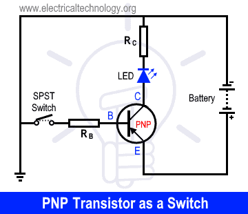
PNP Transistor as a Switch
Semiconductor devices as a whole have found their use in multiple electronic applications. They can be used for either amplification, logical operations, switching, etc. PNP transistor can be used as a switch and is one of its main uses.
PNP transistor when used as a switching device is said to be bipolar transistor. The name bipolar indicates that both the types of charge carriers are used in the working of a bipolar junction transistor.
The working of PNP transistor switching circuit is same like NPN transistor switching circuit expect that current flows from the base. In PNP transistor circuit, the base is always negatively biased with respect to the emitter and this type of switching is used for negative ground configuration.
In PNP transistor switching circuit, the load is connected to the collector terminal as transistor switching output as load. In this configuration, the current flows from the source through the transistor to the load and lastly to the ground. In this switching circuit, the emitter is connected to the consonant voltage source, collector is connected to the load (LED) and then ground while the input is same as PNP i.e. base terminal.
In short,
- If the Base voltage is negative (ground or low) = The Transistor is ON like Closed Switch
- If the Base voltage is Positive (high) = The Transistor is OFF like an Open Switch
Operating Modes of Transistors & Curves
Based on the biasing of the internal diodes of a transistors, the modes of operation when used for switching application can be divided into four modes. These modes of operations are namely cut-off, active, saturation and breakdown regions.
Active Mode
When in this mode of operation, the transistor is often used as a current amplifier. The two diodes in the transistor are in opposite bias, that means one is forward biased and the other is reverse biased. This mode has current flowing from emitter to collector.
Cutoff Mode
When in this mode of operation, both the diodes in the transistor are reverse biased. In this mode, there is no current flow in any direction, and hence the transistor is said to be in OFF state.
Saturation Mode
In this mode of operation, both the diodes in the transistors are forward biased. In this mode, current flows without any restriction from collector to emitter. This happens when the voltage across the base-emitter is high. This mode is said to be the ON state.
Breakdown Mode
When the the value of collector voltage increases beyond the limits, it breakdown the collector diode and the collector current sharply increases to the dangerous level. For this reason, a transistor should not be operated in breakdown region. For example, In 2N3904 transistor, if the value of collector voltage increases more than 40V, the breakdown region starts immediately which leads to damage the transistor circuit.

Applications
- They are used majorly as switches.
- They are used in amplification circuits.
- They are used in darlington (a multi-transistor configuration) pair circuits.
- Recently, they have also been used for robotics.
- PNP transistors are used to control the current flow is electric motors.
- PNP transistors are used to produce the contentious and simultaneous power in matched pair circuits.
Related Posts:
- What is NPN Transistor? Construction, Working & Applications
- Thyristor & Silicon Controlled Rectifier (SCR)
- What is Rectifier? Types of Rectifiers and their Operation
- Electronic Relay Switch Circuit using NPN, PNP, N & P Channels
- Transistor, MOSFET and IGFET Symbols
- Automatic Street Light Control System using LDR & Transistor BC 547
- What is The Difference Between Transistor & Thyristor (SCR)?


How to calculate required filter capacitor in led lighting circuit
Thanks a lot for such a beautiful explanation.
Thanks for the good blog