Push-Pull Amplifier Circuit – Class A, B & AB Amplifier Circuits
Push-Pull Amplifier Circuits using Transistors
A Push-Pull transistor circuit is an electronic circuit that uses active devices connected in a particular way that alternatively supply current and absorb from connected load whenever needed. It used to supply high power to the load. It is also known as Push-Pull Amplifier and in TTL (Transistor Transistor Logic) circuits, it is called “‘Totem Pole Output” based on transistors , diodes and resistors.
A servo amplifiers is used widely because of a special trait that lets them transfer energy to load or even absorb power from the load at times. While the use of these components is extensive, the first choice when it comes to delivering power to these, is a push-pull transistor circuit.
It consists of two transistors in which one is NPN and the other is PNP. One transistor pushes the output on positive half cycle and other pulls on the negative half cycle, hence the name push-pull amplifier. The main advantage of this transistor circuit is that there is no power dissipation at the output transistor, when there is no signal. There are three types of push-pull amplifier but generally, Class-B amplifier is considered as push-pull amplifier.
There are many types of push-pull amplifier circuits but we will consider the following ones related to push-pull amplifier circuits:
- Class A Amplifier
- Class B Amplifier
- Class AB Amplifier
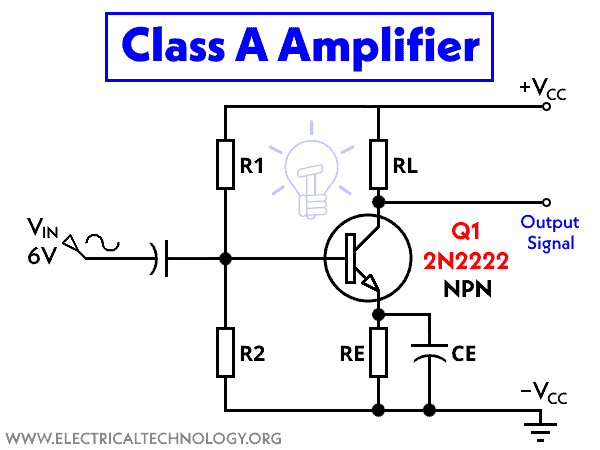
Class A Amplifier
Among the three configurations of the push-pull amplifier, the most common one is Class A configuration. It consists of only one switching transistor that is kept ON always. It is designed such that it gives at its output minimum distortion and maximum amplitude of a signal.
The efficiency of Class A amplifier is very low hovering near 30%. The class A amplifier allows load current to flow through it even though there is no input signal. This causes the amplifier to heat up considerably requiring large heat sinks at the output transistors. The circuit diagram for the Class A amplifier is given below.
Class B Amplifier
Although all the configurations of the push-pull amplifier can technically be called push-pull amplifier, only the Class B amplifier is the actual push-pull amplifier. In contrast to Class A amplifier, Class B amplifier has two transistors for the push-pull electrical action of which one is NPN and the other is PNP.
Each transistor will work for one half of the cycle of the input producing the necessary output. This improves the efficiency of the Class B amplifier many times higher than the Class A amplifier. The conduction angle for this amplifier is 180 degrees, because each transistor works for one half only.
Class B amplifier is one of the most used amplifiers, but it comes with its own shortcoming. It generally suffers from an effect known as Crossover Distortion. Due to this effect, the signal gets distorted at 0V. A transistor requires 0.7V at its base-emitter junction to turn it ON. What that means is that the transistor will not switch ON until the voltage across its base-emitter junction does not reach 0.7V.
The same phenomenon is repeated for the negative half cycle for PNP transistor. This gap in the output when there is no output from the amplifier is called Dead zone. This problem can be solved by using diodes to conduct instead of the transistors when the circuit is in the dead zone. This modified amplifier is now given a different name, it is called Class AB amplifier.
The circuit diagram for a Class B amplifier is given below.

Class AB Amplifier
As discussed above, the crossover distortion defect can be corrected by using two diodes which conduct in transistor’s place. The modified circuit now is known as Class AB amplifier circuit.
This Class AB amplifier is a circuit made using the characteristics of both Class A and Class B amplifier circuits. From 0V to 0.7V the diodes are biased in conduction state where the transistors have no signal at the base terminal. This solves the crossover distortion problem.

Crossover Distortion
Crossover distortion is commonly seen in class B amplifier configurations. The transistors are biased at cut off point in the Class B amplifier. It is known that a silicon transistor and a germanium diode requires 0.7V and 0.2V respectively across its base emitter junction before entering in to conducting mode and this base emitter voltage is called cut-in voltage.
Germanium diodes are out of scope of amplifiers. Transistor can only get the cut-in voltage from the source itself. As a result, portions of the input waveform that are below 0.7 V will be cancelled and so the corresponding portions will be absent in the output waveform. This is called the Crossover Distortion effect.
Now we have the knowledge of Push-Pull amplifiers types and the basic concept behind the working, we will now try to make a Push-Pull transistor circuit ourselves.
Materials Required
- Transformer: (6-0-6)
- PNP Transistor: BC557
- NPN Transistor: 2N2222
- Resistor: 1kΩ
- LED
Transformer (6-0-6)
The transformer that is used in the circuit is a 240V primary windings and center tapped second windings. The transformer acts as step down transformer reducing AC 240V to AC 6V.
Transformer is an electrical device that uses a physical phenomenon called inductive coupling which occurs between two coils of the device to transfer energy between them. These coils in a transformer are called windings. Due to magnetic coupling of the two windings of the transformer, a varying current in one of the coils will produce a resulting change in the other winding.
This occurs due to a magnetic field induced by the varying current in the core of the transformer. This varying magnetic flux induces a varying electromagnetic force or voltage in the secondary winding. The transformer that is used in this circuit has its core made up of high permeability silicon steel, because steel has much higher permeability compared to air or free space which helps in containing the magnetic field that has been produced by the windings. Using these high permeable cores has its own advantages such as a significant reduction of magnetizing current.
BC557 PNP Transistor
BC557 is a very common and widely used PNP transistor. It is a PNP transistor that means that it has the collector and emitter closed when the base pin is kept at ground potential, and will be open circuited when there is a signal at the base terminal. As the BC557 is a general purpose transistor, it can be used to accommodate our needs for a switch.
Due to construction of the transistor, it can not carry loads that draw more than 100mA current. And to switch the transistor from OFF and ON state, the base terminal should be given a current which should not exceed 5mA.
A schematic diagram of the PNP transistor is given below.

The pinout for a BC-557 is given in a tabular form below.
| BC-557 PNP Transistor Terminals | ||
| 1 | Collector | Current flows in through collector |
| 2 | Base | Controls the biasing of transistor |
| 3 | Emitter | Current drains out through emitter |
2N2222 NPN Transistor
The transistor 2N2222 is a general purpose NPN transistor. It is a widely used BJT for general purposes such as switching or low power amplification. The construction of the transistor allows it to be used for applications that require low power operation with moderately high speeds. Along with low power requirement for functioning, it can handle low to medium level of current input and a not very high voltage.
Pin diagram of 2N2222 transistor is given below.

2N2222 NPN transistor pinout is given below. The key features of 2N2222 transistor is to handle the current of higher ratings.
| 2N2222 NPN Transistor Terminals | |
| 1 | Emitter |
| 2 | Base |
| 3 | Collector, connected to case |
Working of Push-Pull Transistor Circuit
In our analysis of the circuit, we will consider the Class B amplifier. The circuit diagram for a Push-Pull amplifier consists of two transistors Q1 and Q2 which are NPN and PNP respectively. When the input signal is positive Q1 starts conducting and produce a replica of the positive input at the output. At this moment, Q2 remains in OFF state. Similarly, when input signal is negative Q1 turns OFF and Q2 starts conducting and produce a replica of the negative input at the output.
Now, why the crossover distortion is happening when Vin reaches zero. Transistor Q1 and Q2 cannot be simultaneously ON. For Q1 to be on we require that Vin must be greater than Vout and for Q2 Vin must be less than Vout. If Vin is equal to zero then Vout must also be equal to zero.
Now when Vin is increasing from zero, the output voltage Vout will remain zero until Vin is greater than Vbe1(which is approximately 0.7V), where Vbe is the voltage required to turn ON the NPN transistor Q1. Hence, the output voltage is exhibiting a dead zone during the period Vin is less than Vbe(=0.7V). this same thing will happen when Vin is decreasing from zero, PNP transistor Q2 will not conduct until the Vin is greater than Vbe2(=0.7V), where Vbe2 is the voltage required to turn ON transistor Q2.
Related Posts
- What is Boost Converter? Circuit Diagram and Working
- 12V to 5V Converter Circuit – Boost and Buck Converters
- How to Make a Voltage Tripler Circuit?
- Simple Overvoltage Protection Circuit using Zener Diode
- MAX232: Construction, Operation, Types and Application
- What is Crowbar Circuit ? Design and Operation


As a technologist, I really appreciate your online tutorial, it further broaden my knowledge in electrical/electronics technology. My difficult experience is how to use digital meter to read or detect faulty components. Do please enlighten.
Your Picture for class B amp seems to be wrong. Both are put as NPN transistors.
The bottom one q1 should have been PNP
We have updated the diagram. Thanks for correction.
Both diagrams (B & AB) above show negative rail, labeled -Vcc, as ground, with the load returning to ground as well. I presume this is just sloppy drafting, as -Vcc and ground are, by definition, not the same thing. A “newbie” might be confused by this.