12V to 5V Converter Circuit – Boost and Buck Converters
12V to 5V Converter Circuit – DC-DC Step Down Conversion
We always do not have a 5V battery readily available, and sometimes we need higher voltage and a lower voltage at the same time to drive different parts of the same circuit. To solve this issue, we use a higher voltage, which is in our case a 12V battery as the main power source and step down this voltage to get a lower voltage, say 5V wherever required. For achieving this, a BUCK CONVERTER circuit is used in many electronic gadgets and applications that drop the voltage to match the load’s requirement.
First, let me tell you about converters. Broadly, there are three types of converters, the first one being Buck converter which steps down the voltage from a higher source voltage. Second, Boost converter, which steps up the voltage from a lower source voltage. In addition, there is another converter which is a combination of the two arranged in some form, the more popular one is Buck-Boost converter which first lowers the voltage and then steps up to the required value. I will try to explain each of the above-mentioned converters in some detail so that the understanding of the upcoming circuitry makes more sense.
- Related Post: Automatic Doorbell with Object Detection By Arduino
What is a Buck Converter?
A buck converter (also known is step down converter) is a DC-to-DC converter, which steps down the voltage from the input to its output. Buck converter achieves its output using semiconductor-switching devices, which are generally diodes and transistors arranged in a particular order and each switched during certain times to finally give the required output. Buck converters can be highly efficient, sometimes often as high as 90%.
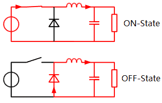
The basic Buck converter circuit consists of the switching transistor, together with the flywheel circuit. When the transistor is in ON state, the current is flowing through the load via the inductor. The inductor opposes changes in the current flow direction also storing energy in the process. The diode, which is connected parallel to the load, is now not operational as it is in the reverse bias.
The current flowing in the circuit also charges the capacitor. Now, when the transistor is turned OFF, the charged capacitor and the inductor apply a voltage across the load because of the back e.m.f. now that there is no voltage source in the circuit. The energy stored in the inductor is sufficient for at least a part of the time the switch is open. If the times for which the switch is kept ON and OFF changes, it, in turn, changes the output DC voltage between 0V and Vin.
The diagram below shows a simple Buck converter operation.
What is a Boost Converter?
Similar to a Buck converter, a boost converter (also known as step up converter) is also a class of switching-mode power supply converters. But the operation of a Boost converter is exactly the opposite of that of a Buck converter. The Buck converter steps down the voltage from a higher supply value to the required value, whereas the Boost converter, steps up the voltage from a lower value of supply.
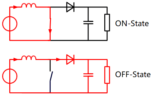
The basic principle of a Boost converter consists of two distinct states. In the first state, the ON state is when the inductor connected to the source side is charged when the switch is ON. Then, when the switch is OFF, the only path offered to the inductor current to flow through is the flyback diode, the capacitor and the load. This results in the transfer of energy which was accumulated in the ON state into the capacitor. If the cycling of the switch is quite fast then the inductor will not discharge fully in between the charging states. Hence the voltage across the load will always greater than that of input source when the switch is OFF.
- Related Post: Smart Home Automation System – Circuit and Source Code
The diagram below shows a simple Boost converter operation.
Buck-Boost Converter
Buck-Boost converter is a type of DC-DC converter. It has greater or less output voltage magnitude than its input voltage magnitude.
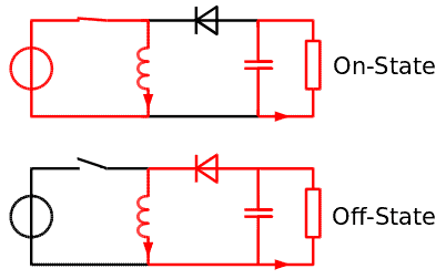
Inverting buck-boost converter having a very basic principle. While in ON state the operation is similar to that of a Boost converter, where the inductor stores energy. A capacitor supplies energy to the load during this time is to connect across the load. While in the OFF state, the inductor is connected to the output load and the capacitor, so the energy stored in the inductor is given to the capacitor and the load. The capacitor gets charged during this time.
Related Posts:
- Half H-Bridge Inverter – Circuit, Operation, Waveforms & Uses
- Full Bridge Inverter – Circuit, Operation, Waveforms & Uses
A simple diagram below shows the working principle of a Buck-Boost converter.
Now, there are many ways to achieve our required BUCK CONVERTER, but we use the most popular switching regulator available in this segment, using the IC MC34063. The other popular method is by using a circuit of MOSFETs switched according to a fixed pattern.
Components Required
- MC34063 switching regulator IC
- 1N5819 schottky diode
- 2k resistors
- 6.2k resistors
- 26 Ohms resistors
- 62 uH inductor, 1.5A
- 100uF, 25V and 359uF, 25V capacitor
- 428pF ceramic disc capacitors
- 12V power supply unit with 1.5A Rating
- Connecting wires
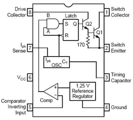
IC MC34063
MC34063 is a monolithic control circuit having all the functions required for the construction of DC-to-DC converters. It consists of multiple functions, which are comparator, oscillator, high current output switch and active peak current limit. MC34063 is available in DIP, SOIC and SON packages. There are eight pins in each. The table of which is given below.
| MC34063 Pinout | ||
| Pin No. | Pin Name | Description |
| 1 | Switch collector | High current internal switch collector input |
| 2 | Switch Emitter | High current internal switch emitter input |
| 3 | Timing Capacitor | Attaching a time capacitor to a variable switching frequency |
| 4 | Ground (GND) | Ground (GND) |
| 5 | Comparator Inverting input | Attach a resistor divider network to build a feedback loop |
| 6 | Voltage (Vcc) | Logic supply voltage |
| 7 | Ipk | Current limit sense input |
| 8 | Driver collector | Darlington pair driving transistor collector input |
Some of IC MC34063 features are as follow:
- Temperature-compensated reference
- Current limit circuit
- Controlled Duty cycle oscillator with an active high current driver output switch
- Accepts 3.0V to 40.0V DC
- Can be operated at 100KHz switching frequency with a 2% tolerance
- Very low standby current
- Adjustable output voltage
Also, this IC is widely available and it is a lot more cost-efficient than the other ICs available in this segment. That is why we are going to use this IC for our circuit.
- Related Post: Car Speed Detector Circuit – Working and Source Code
The pinout of MC34063 is as given below.
There are many applications associated with MC34063, a few of them are Human Machine Interface (HMI), Portable devise, Measurement and test, Gas and blood analyzer, computing, Telecommunications, Cable solutions, etc.
1N5819
The 1N5819 is a metal to silicon power diode, also termed as Schottky Rectifier, which applies the Schottky Barrier Principle. It is mainly used as rectifiers in high-frequency low voltage inverters, polarity protection diodes, and freewheeling diodes. It is also called a surface barrier diode, hot-electron diode or hot carrier diode. It is a little bit different from normal PN junction diodes where metal like platinum or aluminum is used in place of P-type semiconductor. In Schottky diode, semi-conductor and metal joined, forming a metal-semiconductor junction where the semiconductor side acts as a cathode and the metal side acts as an anode. When metal-semiconductor junction formed between metal and semiconductors, they result in a depletion layer also referred to as the Schottky barrier.
Schottky comes with low stored charge and exhibits lower power loss and higher efficiency mechanical characteristics. It is manufactured in such a way that all external surfaces are corrosion resistant and terminals are easily solderable where current flows in one direction only and it stops the current flowing in other direction. The power drop which happens in this diode is lower than PN junction diodes. When voltage is applied across the diode terminals, current starts to flow which results in the small voltage drop across the terminals. The lower voltage drops results in higher efficiency and higher switching speed.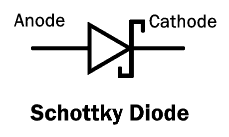
The above schematic diagram shows the electrical symbol for a Schottky diode.
12V – 5V Circuit Diagram
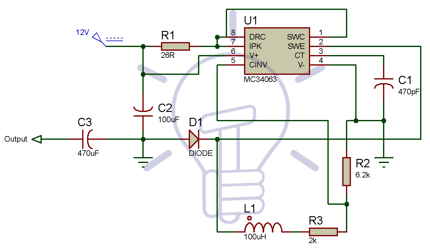
The above circuit diagram shows the circuit along with all the calculated values for our required operation.
Working of 12V to 5V Circuit
Connect the circuit as given in the circuit diagram properly. First to power this chip we connect +V to pin 6 and the pin 4 to ground. At the same time, we connect a capacitor CIN to filter excess noise from the power supply. Pin 3 is connected to CT which is determines the switching speed of the circuit. Pin 5 is the inverting terminal of the comparator. The voltage of the noninverting terminal is 1.25 V from the internal voltage regulator. To the inverting terminal, we place a resistor network composed of two resistors. These decide the gain of the op-amp comparator. In this way, we make a Buck converter which now steps down our input of 12V DC to 5V DC.
Applications
There are many applications in our daily lives, which takes only low-voltage inputs. They also need a regulated 5V for safety. For example, battery chargers, Wi-Fi modules, Arduino modules and so on. The above circuit fulfills the input needs of all of the above mentioned and many more applications.
Related Projects:


Keep up with this program . It’s highly educating .
How to make quality lowpasse filter
It seems to me the circuit is incomplete. Shouldn’t the “output” be connected to the point between L1 and R3 for it to work? C2 looks backwards.
Is it 62uH or 100uH?