How to Make a Voltage Tripler Circuit?
Voltage Tripler Circuit Diagram and Working
What is Voltage Tripler?
Voltage Tripler Circuit is a circuit which triples the input voltage i.e. the output voltage will be three times the peak input voltage. We can build the Voltage Tripler Circuit very easily by using some diodes and capacitors. The voltage tripler circuit is actually a type of multiplier circuits which deliver output voltage two, three or four times of the peak input voltage.
The voltage multiplier circuits are used when we require high voltage and low current. Voltage multipliers are also used to reduce the size of transformer or sometimes remove it. They can be very useful in converting low AC voltage into high DC voltage and low current is needed.
Related Posts:
Components Required
- 3 No. of 1N4007 Diodes
- 3 No. of 22μF Capacitors
- 9-0-9 Step Down Transformer
- Digital Multimeter
Diode (1N4007)
A diode is a unidirectional device i.e. it allows current flow only in one direction. It is used in many electronic applications such as rectifier, signal processing, clipping/clamping of signals, detection of signals, mixing of signals and many electronic systems. It has two terminals Anode and Cathode. So, the current should flow from Anode to Cathode.
Actually, a diode works on the principle of semiconductors. So, there are two types of semiconductors based on free electrons: N-type and P-type.
An N-type semiconductor has a lot of free electrons and very less number of positive holes. So, the electrons are called majority charge carriers and holes are called minority charge carriers. The P type semiconductor has more concentration of positive holes and very less concentration of electrons. So, the majority carriers are holes and minority carriers are electrons.
When P-type and N-type regions come in contact then, majority carriers diffuse from one side to another. As there are fewer holes in the N-type region and fewer electrons in the P-type region, so due to concentration difference electrons move towards the P-type region and holes move towards the N-type region. When the electrons from the N-type region diffuse with holes in the P-type region and holes from the P-type region diffuse with electrons in the N-type region, then a layer of positive ions on the N side and a layer of negative ions on P side appears.
These two layers appear along the junction line of two regions/semiconductors. This region of two layers of ions is known as the depletion region or depletion layer because there is no charge in this region because all of them recombine.
Once the depletion layer is formed, no diffusion of charge carriers from both regions occurs due to the electric field generated from this depletion region.
If we connect the P side of a diode with a positive terminal of battery and N side with a negative terminal, then this is known as forward biasing. If we increase the voltage from zero then in beginning there is no current flowing through the diode, because there is not enough voltage for the charge carriers to cross the potential barrier of the depletion layer. When the voltage applied across the diode is greater than the only current can flow in the diode.
If we connect the N side of a diode with a negative terminal of battery and P side with a positive terminal, then this is known as reverse biasing. When this biasing is applied then the negative electrons in the P side attract towards negative terminal and holes in the N side get attracted towards the positive terminal. As a result of which depletion layer gets wider and hence diode blocks the current. That’s why diode is a unidirectional device.
Related Posts:
- Automatic Bathroom Light Switch Circuit Diagram and Operation
- Simple Overvoltage Protection Circuit using Zener Diode
Capacitor
A capacitor is a device used to store energy in the form of charge. They are widely used in many electronic applications. A capacitor is made up of two metallic plates and there is a dielectric material filled in between it. So when we apply an electric potential across these two plates then an electric field is created between these plates. The positive charge gets collected on the negative side and negative charge gets collected on the positive side.
This process goes on until both the plates have sufficient charges and in that condition, the capacitor is in a fully charged condition. Both the plates have the same charge with different polarities. So an electric field develops between these plates. This is how a capacitor holds the charge. Let us now look at why there is a dielectric-filled between the two plates of the capacitor.
The dielectric is having the molecules which are polar, i.e. they can move towards either of the plates based upon the charge applied on the plates. Hence the molecules align themselves in a way that more electrons can be attracted towards negative plate and more electrons can be repelled out of the positive plate. Now if we remove the battery after charging the capacitor fully, the capacitor can hold this charge for a long time. And this is how it acts as an energy storage element. If you apply a load across the two terminals of the capacitor then it starts discharging and the current starts flowing across the load you have connected.
A capacitor can be used in many places. One of the applications in this project. It can be used as a bypass capacitor too. Bypass capacitors are used with ICs to filter noise in the power supply, like handle the ripples and fluctuations caused due to switching. So when the power supply cuts off at that timing capacitor acts as a temporary power supply. They can also be used in rectifiers. Although the rectifier is made up of diodes but the role of the capacitor is also important.
The output of the rectifier is a continuous waveform which if passed from the capacitor gets converted to a smooth DC signal due to charging and discharging of the capacitor. One more application of the capacitor is in signal filtering. They are used to design the filters which are widely used in signal processing. So they are used in radios to tune the frequency so as to select the perfect channel in which one desires to listen. The last but not the least use of a capacitor is to store energy. Their lifespan is much better than the normal batteries and they can deliver the power much faster as their charging and discharging time is really less.
Related Posts:
- Half H-Bridge Inverter – Circuit, Operation, Waveforms & Uses
- Full Bridge Inverter – Circuit, Operation, Waveforms & Uses
Voltage Tripler Circuit Diagram
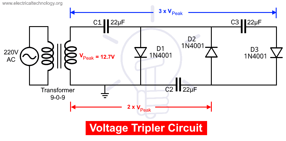 The circuit is really very simple. You can make this circuit either on a breadboard or solder it on Perfboard. You just need to follow the circuit diagram and you are all set. Firstly, connect the transformer’s 9V terminal with the positive terminal of the capacitor. Now, connect the negative terminal of this capacitor to the positive terminal of the diode and then connect this diode’s negative terminal to the 0V terminal of the Transformer. Now, connect another diode’s negative terminal with this diodes positive terminal and positive terminal with the negative terminal of another capacitor’s negative terminal and then connect the positive terminal of this capacitor with 0V terminal of transformer.
Now, you need to connect the third capacitor’s positive terminal with the previous diode’s negative terminal and negative terminal with the third diode’s positive terminal and then connect the negative terminal of this diode with the 0V terminal of the transformer.
We are using a 9-0-9 transformer to step down the AC mains of 220V. Now, in the first positive half cycle, diode D1 gets forward biased and capacitor C1 gets charged from D1 to the peak value of voltage (Vpeak). And, in the negative half cycle, diode D2 is forward biased and diode D1 is reverse biased. D1 does not let discharge the capacitor C1. The capacitor C2 gets charged with the combined voltage of C1 (Vpeak) and negative peak voltage of AC mains, so it gets charged to 2Vpeak.
During the second positive half cycle, diode D1 and D3 conduct and D2 get reverse biased. So, the capacitor C3 charges to the same voltage as C2 which is 2Vpeak. Now, as we can see that the capacitors C1 and C3 are in series so the total voltage across these capacitors is Vpeak + 2Vpeak = 3Vpeak. This is how we get the tripled value of the applied voltage as output. Analytically, the above calculation can be correct. But we have to consider the practical aspect also. Actually, some of the voltage also drops across the diodes, so the output voltage is not exactly thrice of the input voltage. It will be:
Vout = 3 x Vpeak – voltages drop across diodes
Related Posts:
- Buck Converter – Circuit, Design, Operation and Examples
- What is Boost Converter? Circuit Diagram and Working
Working of Voltage Tripler Circuit
The input side voltage will be measured from the transformer and output side voltage will be measured from the third diode. Firstly set the knob of digital multimeter to 20V range and measure the input voltage and then measure the voltage of output side by changing the range. In this project we have used 9V transformer to give the input. This value is RMS value so to determine peak to peak voltage, we need to multiply it with √2, so Vpeak = 9 x √2 = 12.7 V
So analytically our output should be 12.7 x 3 = 38.1 V
But it turns out to be about 37.3 V. So, the voltage drop across diodes is 38.1- 37.3 = 0.8V
Related Posts:


Could a 6X multiplier be used to charge 6ea- 6 volt batteries in parallel and discharge them in series?
For instance,a golf cart?
What would be the output current limitations on the output of such a circuit?
Thanks in advance for all help and advice on this matter.