Simple Overvoltage Protection Circuit using Zener Diode
How to Make an Overvoltage Protection Circuit using Zener Diode?
The electric circuits and components which are used these days give a lot of preference and time to make it as safe as possible. Modern power supplies these days are very reliable, but there is always a chance of failure. A power supply can fail in many ways, but one particularly worrying possibility is that the series regulator element, i.e. transistor or FET may fail in such a way that it becomes a short circuit. This shorting of elements makes a very large voltage appear on the circuitry that is being powered, causing terrible damage to the whole equipment. The damage to the component and to the circuit as a whole can be minimized or completely eliminated by providing a protection circuitry in the form of overvoltage protection.
Short-circuit protection, Reverse polarity protection, and over/under voltage protection are some of the protection circuits that are used to protect any electronic appliance or circuit from any sudden mishappenings. Generally, fuse or MCB is used for overvoltage protection, however in this project, our aim is to make a circuit which can perform better than a fuse or MCB and overcome the limitations of the most primary safety devices mentioned above.
Overvoltage protection is a characteristic of a power supply system, which somehow deals with the voltage across the load side when the input voltage exceeds the pre-set value. In some situations where the input voltage is higher than expected, we always use an overvoltage protection or crowbar protection circuit. The crowbar protection circuit is one of the most used overvoltage protection circuits.
A power supply can fail in many ways; similarly, there can be many ways to protect a circuit from overvoltage. The simplest way is to connect a fuse at the input supply side. But, the disadvantage of using a fuse is that it is one-time protection, because as the voltage exceeds the pre-set value, the fuse wire burns up, causing the circuit to open. Then the only way to get the circuit to start working again is to replace the fuse with a new one and remake all the circuity pertaining to the fuse.
Instances of power supply failure are normally seen as when the power supply stops working and there is no output. However, there are some rare cases of failure, where there is a short circuit and very high voltages may appear at the output. For a linear regulator, we can take the example of a very simple Zener diode based regulator. We can make a more sophisticated circuitry to achieve better results, those circuits use the same idea of passing current through the transistor.
- Related Post: Zener Diode & Zener Voltage Regulator Calculator
The main difference is the way in which the regulator voltage is applied to the base of the transistor. Typically, the voltage at the input side is such that several volts are dropped across the series regulator element. Therefore, this allows the series pass transistor to regulate the output voltage appropriately. Usually a transistor like this would fall in an open circuit condition, but under some circumstances, the transistor may develop short circuit between the collector and emitter. If this occur, then the full unregulated input voltage would appear across the output.
If the full voltage appeared on the output, then it could damage many of the ICs that are in the circuit and are being powered. In this case, the circuit could be well beyond economic repair. The way in which switching regulators work is very different, but there are situations in which the full output could appear on the output of the power supply.
We can make an overvoltage protection circuit using a Zener diode and Bipolar transistor in two methods.
- Related Post: 24V Flasher Circuit
Zener Voltage Regulator Circuit:
this circuit uses a Zener diode to provide a regulated output to the load side, protecting the circuit. But the connections are such that the power flow to the load side is not cut off even when the voltage exceeds the safety limits. The output will always receive a voltage which is dependent on the rating of Zener diode.
Overvoltage Protection Circuit using Zener Diode:
this method is a more straightforward one, wherein the circuit is designed to cut off the power to the load side when the voltage exceeds the given set-values.
Materials Required
- 1N4740A Zener diode
- FMMT718 PNP transistor
- Resistors – 1k, 2.2k and 6k
- 2N2222 NPN transistor
Related Post: Automatic Doorbell with Object Detection By Arduino
Zener Diode
Zener diode is a type of diode that allows current to flow through it in both the directions unlike a normal diode which allow current flow only in one direction which is from anode to cathode. This flow of current in the opposite direction happens only when the voltage across the terminals exceed the threshold voltage called the Zener voltage. This Zener voltage is a characteristic of the device, which governs the Zener effect which in turn governs the working of the diode.
A schematic diagram of a Zener diode generally used in circuits is given below.
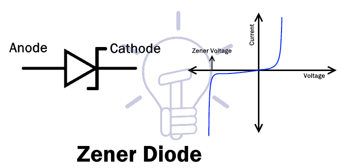
Zener diodes have highly doped p-n junction, which allows the device to function properly even when there is reverse voltage applied through it. However, many Zener diodes rely instead on avalanche breakdown. Both breakdown types occur in the device the only difference being, Zener effect is predominant in lower voltages whereas, the avalanche breakdown happens at higher voltages. They are used to generate low-power stabilized power supplies. They are also used to protect circuits from overvoltage, and electrostatic discharge.
- Related Post: 12V to 5V Converter Circuit
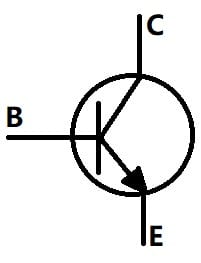
2N2222 NPN Transistor
2N2222 is very common bipolar NPN transistor, mainly used for general purpose low-power amplifying or switching application. 2N222 is designed to operate moderately at high speed. It is a very common transistor and is used as an exemplar of an NPN transistor.
The schematic diagram of the transistor is given below.
The pinout for 2N2222 NPN transistor is given below.
| 2N2222 | |
| 1 | Emitter |
| 2 | Base |
| 3 | Collector, connected to case |
Due to the low cost and small size, it is the most commonly used transistor. One of its key features is its ability to handle the high values of currents compared to the other similar small transistors. It is either made up of silicon or germanium material and doped with either positively or negatively charged material. While performing amplification applications, it receives an analog signal via collectors and another signal is applied to its base. Analog signal could be the voice signal having the analog frequency of almost 4kHz (human voice).
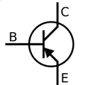
FMMT718 PNP Transistor
FMMT718 is a PNP transistor hence the collector and emitter will be closed (Forward biased) when the base pin is held at ground and will be opened (reverse biased) when a signal is provided to base pin. This is where PNP transistor differs from a NPN transistor; a logic gate is used to toggle between ground signal voltages.
A schematic diagram of the PNP transistor is given below.
The pinout for a FMMT718 is given in a tabular form below.
| FMMT718 | ||
| 1 | Collector | Current flows in through collector |
| 2 | Base | Controls the biasing of transistor |
| 3 | Emitter | Current drains out through emitter |
Zener Voltage Regulator Circuit
This is one of the two configurations of overvoltage protection circuits using Zener diode. This circuit not only protects the load side circuit but also regulates the input supply voltage to maintain a steady voltage. Circuit diagram for Overvoltage protection using Zener voltage regulator circuit is given below.
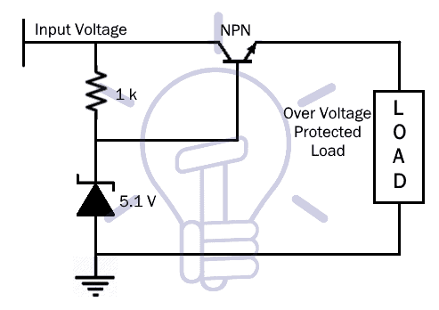
The threshold voltage above which the circuit disconnects the supply to the load side is called the circuit’s pre-set voltage value. The design of the circuit is such that the pre-set value of the circuit is the rating of the Zener diode. So the threshold value over which the circuit does not conduct is approximately 5.1V.
The conduction of the transistor Q1 is dependent on the base emitter voltage of the transistor. When the circuit’s output voltage starts to raise, this increases the Vbe of the transistor and it conducts less. This in turn reduces the output voltage, keeping the output voltage almost constant.
Circuit Diagram of Overvoltage Protection using Zener Diode
The circuit diagram for the Overvoltage protection circuit is given below.

First, we consider the working of the circuit when the power supply is working properly. In proper working state, the base terminal of transistor Q2 is high which causes that transistor to turn OFF. When Q2 is turned OFF, the transistor Q1’s base terminal is low and it starts conducting. In this way the load is connected to the supply when the supply voltage is below the set threshold voltage.
Now, when the voltage supply is higher than the threshold value, Zener breakdown happens and the Zener diode D2 starts conducting. This makes the base terminal of Q2 which was earlier high to ground. Now that the base terminal of Q2 is connected to ground, it starts conducting. The base of the transistor Q1 which is connected to the output of the Q2 is now high and it stops conducting. This isolates the load from the supply saving it from any potential damage that could have caused due to the voltage surge.
The working of the circuits given above is also dependent on the voltage drop of each transistor. Ideally, it should be low for a circuit to match its theoretical counterpart. To keep the voltage drop for the transistor to a minimum, we have used FMMT718 PNP transistor which has a very low collector emitter saturation value. This low value of Vce allows of the drop in the voltage across the transistors low.
Related Posts:


Fascinating and interesting site!
Good Day, I am currently doing my Final year engineering project, and would like to use the overvoltage circuit displayed on the website in my design. Would it be possible for me to receive formal consent for making use of this circuit within my report and obviously reference the post? Kind regards JJ Link to pose in question: https://www.electricaltechnology.org/2019/11/simple-overvoltage-protection-circuit-using-zener-diode.html