Bipolar Junction Transistor (BJT) | Construction, Working, Types & Applications
BJT – Bipolar Junction Transistor – Construction, Working, Types & Applications
History
Bipolar junction transistor (BJT) was invented by William Shockley and John Bardeen. While the first transistor was invented 70 years ago but till now it changed the world from mysterious big computers to small smartphones. The invention of transistor changed the concept of electrical circuits to integrated circuits (IC). Nowadays, the use of BJT is decreasing because CMOS technology took place in the design of digital ICs.
What is BJT – Bipolar Junction Transistor?
Bipolar junction transistor (BJT) is a bidirectional device that uses both electrons and holes as charge carriers. While Unipolar transistor i.e. field effect transistor uses only one type of charge carrier. BJT is a current controlled device. The current flows from emitter to collector or from collector to emitter depending on the type of connection. This main current is controlled by a very small current at the base terminal.
Construction
Bipolar junction transistor is formed by the combination of two back-to-back doped semiconductor materials. In other words, BJT is formed by the “sandwich” of back to back extrinsic semiconductor materials. These extrinsic semiconductors are PN junction diodes. Two PN junctions’ diodes are sandwiched together to form a three-terminal device knows as BJT transistor. BJT is a three-terminal device having two junctions.
After doping an intrinsic semiconductor with Trivalent or Pentavalent impurities a P-type semiconductor or N-type semiconductor respectively is made. If the number of electrons are greater than the number of holes (positive carriers) then that is known as N-type semiconductor material. While in P-type semiconductor, the number of holes is greater than the number of electrons. When P-type and N-type material are connected together then it becomes a PN-junction diode. BJT transistors are formed after connecting two PN junctions back to back. These transistors are known as PNP or NPN bipolar junction transistors depending on whether P or N-type is sandwiched.
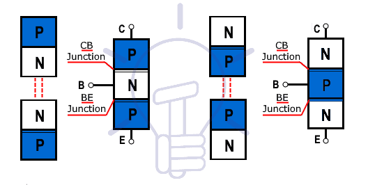
Basically, transistors have three portions and two junctions. These three portions are called Emitter, Collector, and Base. The emitter and collector sandwich the base in between them. The middle portion (base) forms two junctions with the emitter & collector. The junction of the base with emitter is known as the Emitter-Base junction while the junction of the base with the collector is known as the Collector-Base junction.
Terminals of BJT
There are three terminals of BJT. These terminals are knowns as collector, emitter and base. These terminals are briefly discussed here.
Emitter
The emitter is the portion on one side of the transistor which emits electrons or holes to the other two portions. The base is always reverse bias with respect to emitter so that it can emit a large number of majority carriers. It is the most heavily doped region of the BJT. The emitter-base junction should be always forward bias in both PNP and NPN transistors. Emitter supplies electrons to the emitter-base junction in NPN while it supplies holes into the same junction in PNP transistor.
Collector
The portion on the opposite side of the Emitter that collects the emitted charge carriers (i.e. electrons or holes) is known as collector. The collector is heavily doped but the doping level of the collector is in between the lightly doping level of base and heavily doped level of emitter. Collector-base junction should be always reversed biased in both PNP and NPN transistors. The reason for reverse biasing is to remove charge carriers (electrons or holes) from the collector-base junction. The collector of NPN transistor collects electrons emitted by emitter. While in PNP transistor, it collects holes emitted by emitter.
Base
The base is the middle portion between collector and emitter & it forms two PN junctions between them. The base is the most lightly doped portion of the BJT. Being the middle portion of the BJT allows it to control the flow of charge carriers between emitter and collector. The base-collector junction shows high resistance because this junction is reversed bias.
Type of BJT
This three-layer device formed by back to back connection has specific names. It can be weather PNP or NPN. Both connections are disused here briefly.
PNP Construction
In PNP bipolar transistor, the N-type semiconductor is sandwiched between two P-type semiconductors. PNP transistors can be formed by connecting cathodes of two diodes. The cathodes of the diodes are connected together at a common point known as base. While the anodes of the diodes that are on the opposite sides are known as the collector and the emitter.
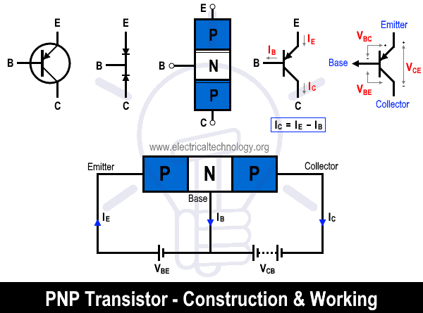
The emitter-base junction is forward bias while collector-base junction is reverse bias. So, in PNP type current flows from emitter to collector. The emitter, in this case, is at high potential to both collector and base.
NPN Construction
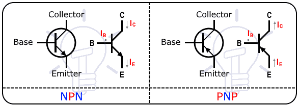
NPN type is exactly opposite to PNP type. In NPN bipolar transistor, the P-type semiconductor is sandwiched between two N-type semiconductors. When the anodes of two diodes are connected together it forms an NPN transistor. The current will flow from the collector to emitter because the collector terminal is more positive than emitter in NPN connection.

The difference between PNP and NPN symbol is the arrow mark at the emitter which shows the direction of flow of current. The current will either flow from emitter to collector or from collector to emitter. The arrow mark in PNP transistor is inward, which shows the flow of current from emitter to collector. In case of NPN collector, the arrow mark is outward, which shows the flow of current from collector to emitter.
Related Post: What is NPN Transistor? BJT Construction, Working & Applications
Working of BJT
The word “transistor” is the combination of two words, “Trans” (Transform) and “istor” (Varistor). So, it means the transistor can transform its resistance. The resistance varies in such way that it can either act as an insulator or conductor by applying small signal voltage. This changing ability makes it able to perform both as an “Amplifier” or a “Switch”. It can be used either as a switch or an amplifier at a single time. Therefore, BJT can operate in three different regions to perform the said operation.
Active Region:
In Active region, one of the junctions is in a forward bias while the other is in reverse bias. Here, the base current Ib can be used to control the amount of collector current Ic. Therefore, the active region is used for amplification purposes where the BJT acts as an amplifier with a gain β using the equation;
ic = β x Ib
It is also known as linear region. This region is in between the cutoff region and the saturation region. The normal operation of BJT occurs in this region.
Saturation Region:
In saturation region, both of the junctions of the BJT are in forward bias. This region is used for the ON-state of a switch where;
ic = isat
Isat is the saturation current & it is the maximum amount of current flowing between emitter and collector when BJT is in saturation region. Since both junctions are in forward bias so, BJT acts as a short circuit.
Cutoff Region:
In cutoff region, both junctions of a BJT are in reverse bias. Here the BJT work as off state of a switch where
ic = 0
The operation in this region is completely opposite to the saturation region. There are no external supplies connected. There’s no collector current and hence no emitter current. In this mode, transistor acts as an off-state of the switch. This mode is achieved by reducing base voltage less than both emitter and collector voltage.
Vbe < 0.7
Working Principle of BJT
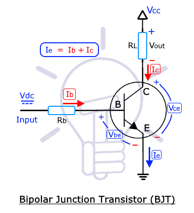
BJT have two junctions formed by the combination of two back to back PN junctions. Base-Emitter junction (BE) is forward bias while collector-emitter junction (CE) is reverse bias. At BE junction, the potential barrier decreases with forward bias. So, electron start flowing from emitter terminal to base terminal. As the base is lightly doped terminal, so very little number of electrons from emitter terminal combine with holes in base terminal. Due to combination of electrons and holes, current from base terminal will start flowing known as Base current (ib). Base current is only 2% of the emitter current Ie while the remaining electrons will flow from the reverse bias collector junction known as Collector current (ic). The total emitter current will be the combination of base current & collector current given by;
ie = ib+ic
Where ie is approximately equal to ic because Ib is almost 2% of the IC.
BJT Configuration
BJT is three-terminal device so there are three possible ways to connect BJT in a circuit with one terminal being common among others. In other words, one terminal is common between input and output. Each connection responds differently to input signal as shown in the table below.
| Configurations | Voltage Gain | Current Gain | Power Gain | Input Impedance | Output Impedance | Phase Shift |
| Common base configuration | High | Low | Low | Low | Very high | 0 degree |
| Common emitter configuration | Medium | Medium | High | Medium | High | 180 degree |
| Common collector configuration | Low | High | Medium | High | Low | 0 degree |
Common Base Configuration:
In common base configuration, the base terminal is common between the input and output signals. The input signal is applied between base and emitter terminal while output is taken between the base and collector terminal.
The output signal at collector side is less than the input signal at emitter. So, its gain is less than 1. In other words, it “attenuates” the signal.
It has a non-inverting output that means that both input and output signals are in-phase. This type of configuration is not commonly used because of its high voltage gain.
Due to its very high-frequency response, this configuration is used for single stage amplifier. These single stage amplifiers can be used as radio frequency amplifier, microphone pre-amplifier.
Common Base Configuration Gains
| Voltage Gain |  |
| Current Gain | Ic/ie |
| Resistance Gain | RL/Rin |

Common Emitter Configuration
As its name suggests, in common emitter, the emitter is common between input and output. The input is applied between base & emitter while output is taken between collector & emitter. It can be simply recognized by looking at the circuit. If the emitter is grounded while input and output are taken from the base and collector respectively.
This configuration has the highest current and power gain among all three configurations. The reason is because the input is at forward bias junction, so its input impedance is very low. While output is taken from reverse bias junction, so its output impedance is very high.

The emitter current in this configuration is equal to the sum of base and collector currents. Given in equation as;
Ie= ic + ib
Where ie is the emitter current
This configuration has high current gain which is ic/ib. The reason for this tremendous current gain is that the load resistance is connected in series with collector. It can be seen from the equation that minute increase in base current will result in extremely high current at output side.
This configuration acts as an inverting amplifier where the output signal is completely opposite in polarity to the input signal. Therefore, it shifts the output signal at 180° with respect to its input signal.
Common Collector Configuration
Common collector configuration known as voltage follower or emitter follower has a grounded collector. In Common collector configuration, the collector terminal is grounded to the supply. So the collector terminal is common to both input and output. The output is taken from the emitter terminal with load connected in series while the input is given to base terminal directly.
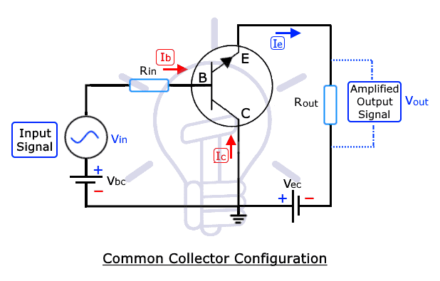
It has high input impedance and low output impedance. This enables it to perform as an impedance matcher. So, this configuration is very helpful in the impedance matching technique.
BJT Biasing
The process of setting the transistor DC voltage or current levels such that to achieve proper amplification of the applied AC input signal. By elaborating further, biasing is the technique using for preventing the transistor to work either in cutoff mode or saturation mode.
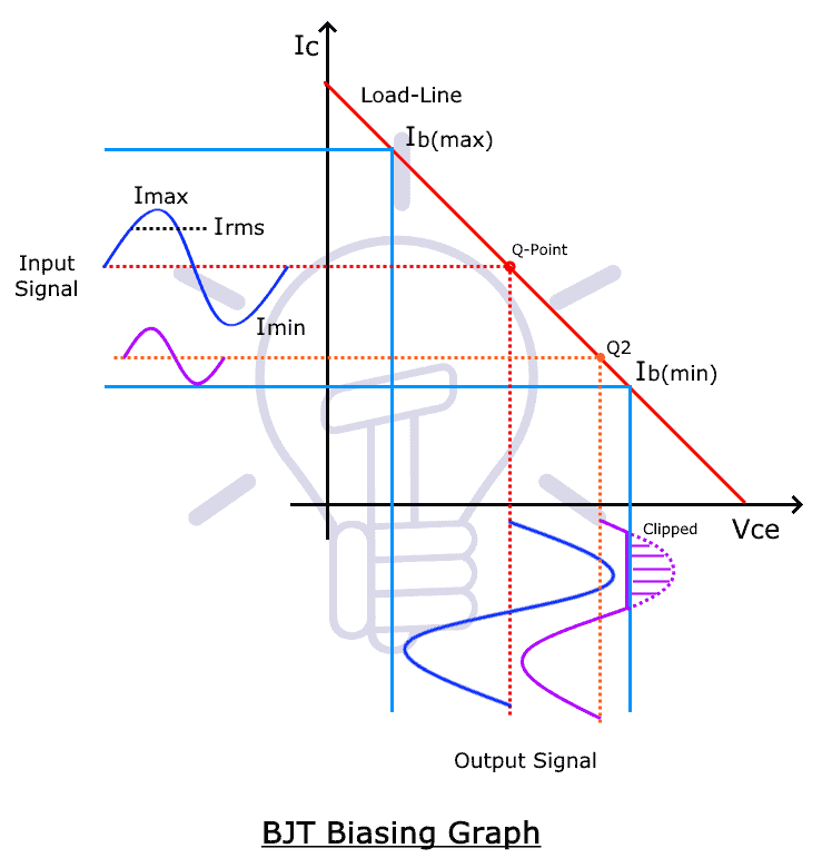
To retain output signal without any loss after amplification, proper biasing is a must. The operation of steady-state in mainly dependent on collector current (ic), base current (ib) and collector to emitter voltage (Vce). If the transistor is meant to operate properly as an amplifier. Then these parameters must be chosen correctly which is known as biasing of transistor. The aim of the transistor biasing is to achieve a known quiescent operating point or Q-point for BJT to produce an undistorted output signal. Q2 given in the above graph is not a proper q-point & it causes to clip the upper portion of the output signal.
Types of Biasing
Without biasing the transistor will work as an insulator or conductor. So, for proper amplification purpose BJT is biased through different techniques. Though there are many different techniques, but few most common techniques are discussed briefly.
Fixed Bias
A single power supply is used for both collector and base. In the fixed bias configuration, the base current of the BJT remains constant irrespective of input DC voltage (Vcc). This depends on selecting the resistor such that to keep the Q-point fixed and hence known as fixed biased configuration. The value of bias resistor can be found by
(Vcc-Vbe) / Ib.
where Vbe=0.7v for standard transistors and
Ib = Ic / β.

Advantages of Fixed Bias
Some of the advantages of this circuitry are discussed.
- No loading effect: There’s no loading effect. Where the loading effect can be defined as the effect of the load on the source. By using this circuitry for biasing, we can get rid of the reducing level of voltage of the voltage source.
- Simple circuit: Its circuit is very simple because it only requires one fixed resistor RB.
- Easy calculation: The calculation method is very simple.
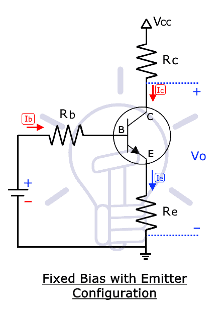
Fixed Bias with Emitter Resistance
It is the modified form of fixed biased circuit where external resistance is connected to the emitter terminal. This circuit requires an extra resistor for emitter which provides negative feedback.
The bias voltage VBB-VBE = IBRB + IERE should appear across RE to set IE≈Ic.
Circuit of Fixed bias with emitter resistance
Advantages of Fixed Bias with Emitter Configuration
- No thermal Runaway: The deficiency of thermal run away in fixed bias can be overcome with fixed bias with emitter resistance configuration. Thermal runaway can be defined as the increase in collector current with an increase in temperature. This causes self-destruction because the overcurrent cause overheats.
- The problem with this configuration is that it reduces the gain of BJT amplifier. This problem can be overcome very easily by bypassing emitter resistance.
Collector to Base Bias
Base resistor is connected to the collector terminal in this type of biasing. This configuration stabilizes the operating point and preventing thermal runaway by employing negative feedback. This configuration is also the improved version of the fixed bias configuration. The biasing resistor is connected between collector and base which provide feedback path. Collector to base bias is an improved technique over fixed bias technique.
This configuration is also known as voltage biased feedback circuit. Because Rb directly appears across output and input. In other words, a part of output is feedbacked to input. So negative feedback exists in the circuit.
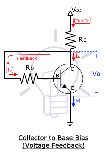
If there is a change in beta due to piece-to-piece-variation or the temperature rise in beta and Ico, then collector current tries to increase further due to which the voltage drop across Rc increases. As a result, Vce and Ib decreases. Therefore, the final value of the collector value Ic is maintained stable by the circuit, which keeps the Q point fixed.
This circuit is also known as Voltage Feedback Bias circuit because Rb appears directly across input and output in this circuit. increase in collector current decreases the base current.
Voltage Divider Bias or Potential Divider
Two external resistors R1 and R2 are used for this type. The voltage across R2 forward biases the emitter junction. With the proper selection of R1 and R2, the operating point of the transistor can be made independent of Beta. Potential divider bias is the most popular and used method for biasing of transistor. The emitter diode is forward biased by controlling the voltage drop at R2.
Rb = R1 || R2
In the voltage divider bias circuit, the value of Rb is equal to the parallel combination of R1 and R2.
Circuit of voltage divider bias:

Advantage of Voltage Divider Bias
Independent of beta: The main advantage of voltage divider bias circuit is that the transistor will be no more dependent on beta. The reason is that the terminal’s voltages of transistor i.e. collector, emitter, and base voltages will be dependent on the external circuit. Emitter Resistance Re allows the stability of the gain despite fluctuations in beta.
Limitations of BJT
Here are some limitations of Bipolar junction transistor;
- Bulky: BJTs are bulky which require more space and hence very rarely used in integrated circuits (IC) fabrications.
- Low switching Frequency: its switching time is very low which is another reason for rarely been using in IC As compare to MOSFETs the frequency is very low
- Leakage current: leakage currents with BJTs are enough so they can’t be used for high frequency.
- Thermal stability of BJT: compared to other transistors, the thermal stability of BJT is very low and it is a noisy device.
- Thermal runaway: BJT suffers from thermal run-away problem which results in excess heat produced. In other words, it causes self-destruction. As the heat produces is equal to I2 So, the excess current will cause excessive heat which will burn the BJT.
- Early effect: The emitter to collector current is controlled by base current. If the base width is moved to zero known as punch through, then the junction of collector and emitter touches each other. After that a tremendous current starts flowing from emitter to collector which cannot be controlled by base current. This out of control is known as early effect and is one of the main limitations among limitations of BJT.
Vulnerability
Radiation damage causes to transistor when transistors are exposed to ionization radiation. The minority carrier’s lifetime reduces after exposure to radiation, which causes gradual loss of gain of the transistor.
Transistor has power ratings and reverse breakdown voltage beyond which the BJT may fail to work. When BJTs are operated beyond their power rating or reverse breakdown voltage then BJT will not work properly or may be damaged permanently.
In case of reverse biasing, the emitter-base junction will cause avalanche breakdown which will permanently damage the current gain of the bipolar junction transistor.
Advantages of BJT
- Large gain bandwidth: Gain bandwidth is the difference between maximum & minimum cutoff frequency. The gain at the cutoff frequency is 0.7. By further increasing or decreasing the frequency from maximum & minimum cutoff frequency respectively, the gain decreases, which is not usable. So BJT offers a wide range of frequency offering a greater gain then 0.7. Therefore, the BJT has a tremendous gain bandwidth.
- Low forward voltage drops: BJTs have 0.6v of forward voltage drop which is very low and quite important point. The point is of great significance because more forward voltage will cause unnecessary power loss according to P=VI. It means that for the same type of load, a device having high forward voltage drop will cause unnecessary power loss.
- Darlington pair: Due to its low output impedance and high input impedance, BJT can provide meritorious current gain.
- Long life: BJTs have relatively long life of operation. The device gets festered because the saturation current increases with the passage of time. While different techniques of biasing may be used to overcome this problem and increase the life of the device further.
Related Posts: What is The Difference Between Transistor & Thyristor (SCR)?
Application of BJT
Here are some of the applications of Bipolar Junction Transistor;
- Converters: BJTs can be used in vast majority of converters. These converters can be of different types such as inverters, buck converters, boost converters or any DC-DC, DC-AC, AC-DC or AC-AC
- Temperature sensors: Finding temperature is one of the other applications of BJT. Where this can be found by two voltages at two different levels in a known ratio are subtracted
- High driving capability: It has High driving capability. For high voltage or current-handling capability, devices are connected in series and in parallel correspondingly. But the driving capability of individual devices is always considered.
- High-frequency operation: BJTs can be operated on a very high frequency. The frequency of the BJT for small signal is much higher than its switching frequency, principally due to storage delay. The storage time of 2N2222 is 310ns, thus the maximum switching frequency is about 3MHZ.
- Digital switch: The digital logic family has emitter-coupled logic used in BJTs as a digital switch.
- Oscillation circuit: These are preferred in oscillation circuits.
- Clippers: BJTs can be used in clipping circuits for changing the shape of waves. This can be used as a simple diode for clipping purpose but the problem with diode is that diode is uncontrolled.
- Demodulator and modulator: BJTs can be used in demodulation and modulation circuits. BJTs are still using in the very old known modulation technique known as “Amplitude modulation”.
- Detection circuits: BJTs can be used in detector circuits. BJT could be a new semiconductor sensor type for measuring ionization radiation dose.
- Amplifiers: One of the most important applications of BJTs is amplification where it is used in amplifier’s circuit to amplify small signals. such as in audio amplifiers, these tiny components amplify very low audio signal to hearable range.
- Electronic switches: It can be used as an electronic switch. BJTS are used in inverter for changing the direction of DC current and become AC current.
- Automatic switch: It can be used instead of manual switch in an electrical circuit. the output signal of sensors is sometimes useless in electrical circuits because these signals are very low. However, these signals will become useful if they drive BJTs. As BJT operates on low signals. Then these BJT switches can run heavy loads including motors.
Related Posts:
- How to check the PNP and NPN transistor values through DMM
- Thyristor & Silicon Controlled Rectifier (SCR)
- Rectifier -Types of Rectifiers and their Operation
- Types of Diodes and Their Applications
- What is a Sensor? Different Types of Sensors with Applications
- Electronic Relay Switch Circuit using NPN, PNP, N & P Channels
- Types of Computer Memory with their Applications
- Transistor, MOSFET and IGFET Symbols