What is Diode? Construction & Working of PN Junction Diode
Diode Construction, Working, Types, VI Characteristics, Advantages & Applications
What is a Diode?
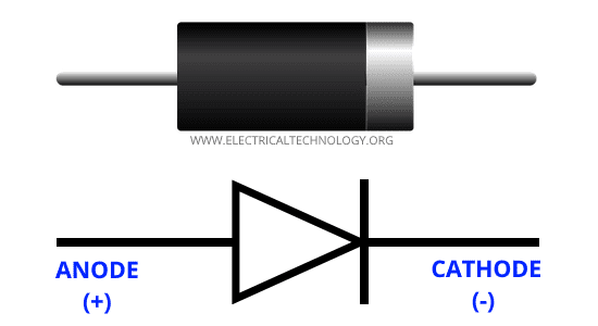
“Di “= Two, and “Ode “= Electrodes i.e a device or component having two electrodes viz Anode “+” (P) and Cathode “-” (N).
A diode is a two-terminal unidirectional power electronics device. The semiconductor diode is the first invention in a family of semiconductor electronics devices. After that many types of diodes are invented. But today also the most commonly used diode is a semiconductor diode.
Generally, silicon is used to make a diode. But another semiconductor material like germanium or germanium arsenide is also used.
A diode allows current to flow only in one direction and it blocks the current in another direction. It offers low resistance (ideally zero) in one direction and it offers a high resistance (ideally infinite) in another direction.
Symbol of Diode
- Related Post: Different types of Diodes Symbols
Construction of Diode
There are two types of semiconductor material; Intrinsic and Extrinsic semiconductor. An intrinsic semiconductor is a pure semiconductor in which hole and electrons are available in equal numbers at room temperature. In an extrinsic semiconductor, impurities are added to increase the number of holes or the number of electrons. These impurities are tri-valent (boron, indium, aluminum) or pentavalent (phosphorous, Arsenic, Antimony).
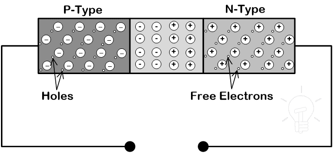
A semiconductor diode has two layers. One layer is made of a P-type semiconductor layer and the second layer is made of an N-type semiconductor layer.
If we add trivalent impurities in silicon or germanium, a greater number of holes are present and it is a positive charge. Hence, this layer is known as the P-type layer.
If we add pentavalent impurities in silicon or germanium, a greater number of electrons are present and it is a negative change. Hence, this layer is known as the N-type layer.
The diode is formed by joining both N-type and P-type semiconductors together. This device is a combination of P-type and N-type semiconductor material hence it is also known as PN Junction Diode.
A junction is formed between the P-type and N-type layers. This junction is known as PN junction.
A diode has two terminals; one terminal is taken from the P-type layer and it is known as Anode. The second terminal is taken from the N-type material and it is known as Cathode.
The below figure shows the basic construction of the diode.
![]()
- Related Post: Thyristor & Silicon Controlled Rectifier (SCR)
Working of Diode
In the N-type region, electrons are the majority charge carriers and holes are minority charge carriers. In the P-type region, the holes are majority charge carrier and the electrons are negative charge carriers. Because of the concentration difference, majority charge carriers diffuse and recombine with the opposite charge. It makes a positive or negative ion. These ions are collected at the junction. And this region is known as the depletion region.
When anode terminal of diode is connected with a negative terminal and cathode is connected with the positive terminal of a battery, the diode is said to be connected in reverse bias.
Similarly, when anode terminal is connected with a positive terminal and cathode is connected with the negative terminal of the battery, the diode is said to be connected in forward bias.
Operation of Diode in Reverse Bias Condition
The diode is connected in reverse bias. In this condition, free electrons diffusing into the P-type regions and recombine with holes. It will create negative ions. Similarly, holes diffuse into the N-type region and recombine with electrons. It will create positive ions.
The connection diagram is as shown in the below figure.
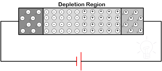
When such voltage is applied to the circuit, immobile ions create a depletion region as shown in the above figure. The width of the depletion region is large. Hence, no more hole or electron crosses the junction.
It cannot create a flow of electrons or holes even if it is supplied at rated voltage. Hence, it is not possible to flow the current through the diode and it behaves as an open switch.
Here a very small amount of current will flow through the circuit. This current is known as reverse saturation current or reverses leakage current. This current flow due to the minority charge carriers. This current is not high enough to conduct the diode.
If we increase the voltage up to reverse breakover voltage, the minority charge carriers get high kinetic energy and collide with atoms. In this condition, the number of covalent bonds broken and a huge number of electrons-holes pair generates a huge amount of flow of current.
Due to this high amount of current, a diode may get damaged. Hence, in general condition, the diode is not connected in reverse bias.
Operation of Diode in Forward Bias Condition
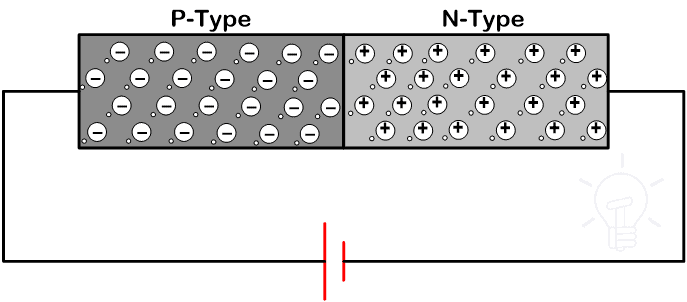
When the anode is connected with the positive terminal of the battery and cathode is connected with a negative terminal of the battery, the anode is positive with respect to the cathode. And the diode is said to be connected in forward bias.
Now, we gradually increase the supply voltage. If we increase a small voltage, the majority charge carrier does not get sufficient energy to cross the depletion region.
In the forward bias conditions, the width of the depletion region is very small. If we increase the voltage more than forward breakover voltage, the majority charge carrier gets enough energy to cross the depletion region.
For silicon forward breakover voltage is 0.7V and for germanium forward breakover voltage is 0.3V.
When supply voltage increases more than this voltage, the majority charge carriers flowing through the circuit and it made the diode conducting.
In this mode of operation, a very small amount of drop occurs. This drop is known as an on-state voltage drop. The connection diagram of this mode is as shown in the below figure.
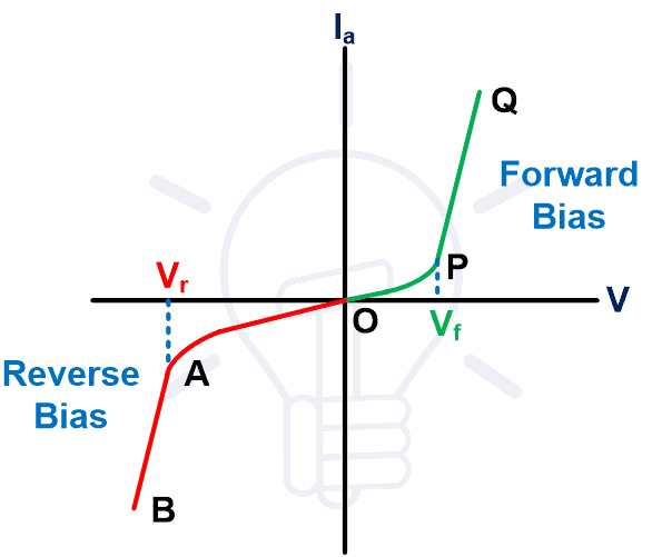
VI-Characteristics of Diode
The VI characteristic of the diode shows the relation between diode current and voltage. It is a graph between voltage and current where the voltage is on X-axis and current is on Y-axis.
The circuit diagram to obtain the VI characteristic of the diode is as shown in the below figure.
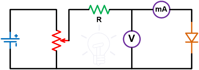
The characteristic is divided into two parts;
- Forward Bias
- Reverse Bias
When voltage is not applied, the current flowing through the circuit is zero. The point ‘O’ shows this condition where voltage and current are zero.
Forward Bias
When the P-type material or anode is connected with the positive terminal of the battery and N-type material or cathode is connected with a negative terminal of a battery, then the diode is connected in forward bias.
The applied voltage is controlled by the variable resistor. The applied voltage is gradually increased. The current will not flow until the voltage increases forward breakover voltage. Because in this condition, the voltage is not sufficient to move charge carrier from one layer to another.
For silicon, breakover voltage is 0.7V and for germanium, this voltage is 0.3V. Once the voltage is increased above this level, the voltage is sufficient to move charge carrier from one carrier to another carrier. And due to the flow of charge, current can flow through the diode.
As shown in characteristics, part OP is the non-linear part. That shows the starting period where voltage is below forward breakover voltage. Here, the current is very small.
The part PQ shows when the voltage is more than the forward breakover voltage. And in this condition, the current increases linearly.
In this condition, the diode behaves as a close switch as it allows the current to flow. For the ideal diode, the on-state resistance is zero and It behaves as a pure conductor.
Reverse Bias
In reverse bias, the N-type material or cathode is connected with a negative terminal of the battery. This type of connection is known as a reverse bias connection.
In this condition, the voltage is gradually increased with the help of a variable resistor. But this voltage is not sufficient to cause the flow of current.
Because the junction created between P-type and N-type layer is in reverse bias and the depletion width is large in this condition. Therefore, the rated voltage is not sufficient to create a movement of charge carrier.
Hence, the current will not flow through the diode. The curve obtains in this mode is OA. As shown in the graph, a very small amount of current will flow due to the minority charge carrier, this current is not sufficient to turn ON the diode.
When the applied voltage is more than the reverse breakdown voltage, a large current will flow due to the avalanche breakdown. This part is shown as AB in the graph.
Types of Diodes
There are different types of diodes and we have explained each type of diode in very detail in the previous post. You may refer to the 24 types of diodes article.
Advantages of Diodes
There are some advantages of PN junction diodes over vacuum diodes as follow.
- Small in size
- less space required
- low in weight
- Most Reliable in operation
- Consume low power
- Better life span and efficiency
- Low internal resistance
- Easy Installation and maintenance
- Simple construction and strong
- low cost and easy availability
Applications of Diodes
Diodes are used in various applications in power electronics. The diode is a unidirectional two-terminal device that only allows flowing the current in one direction and blocks the current in another direction. Due to this characteristic, the diode is used in the application like;
- Rectifier
- Voltage multiplier circuit
- Over-voltage limiter
- Clipper and clamper circuit
- Reverse current protection circuit
- Digital Logic gates
- It is used in solar panels to avoid the flow of current in a reverse direction and used to bypass the solar plate.
- It is also used to modulate and demodulate communication signals.
There are many other types of diodes are available that is made for the several types of diode like;
- The photodiode is used for the conversion of photon energy into electrical energy.
- Light Emitting Diode is used for illumination purposes.
- Zener diode is used as a voltage regulator circuit.
- A tunnel diode is used for the RF circuit.
- A variable capacitance diode is used for tuning purposes.
Related Posts:
- How to Test a Diode using Digital & Analog Multimeter? – 4 Ways.
- Blocking Diode and Bypass Diodes in a Solar Panel Junction Box
- Simple Overvoltage Protection Circuit using Zener Diode
- Zener Diode & Zener Voltage Regulator Calculator
- PNP Transistor – Construction, Working & Applications
- NPN Transistor – Construction, Working & Applications


Hello. I have a query regarding the reverse biased capacitance of a diode with temperature change. I understand that in reverse biased a diode will look like a capacitor. The value will be based on the type of diode and the reverse voltage applied. I get all that but for a given reverse voltage and a given diode what happens to the capacitance with temperature change? For instance how does a 1N914 diode capacitance with a given set reverse voltage vary with temperature changes?. I have seen nothing noted in any data sheet so far?
regards
Harry