Digital Latches – Types of Latches – SR & D Latches
Types of Digital Latches, Construction & Applications
What is Digital Latch?
A sequential logic circuit or electronic device used for storing binary information is known as Latches. Latches are bi-stable multi-vibrator; it means that latches have 2 stable states, LOW and HIGH.
It stores the information provided to it in binary form and does not need a constant input.
The latches are level sensitive i.e. they operate on logic’s level & flip-flops are edge sensitive i.e. they operate on clock edges.
Latches change its state whenever the input logic level changes considering the latch is enabled first. However, flip-flops do not change its state with a change in input’s logic until there is an edge of controlling signal. The simplest latch is S-R Latch
Difference Between Latches and Flip Flops
Both Latches and flip flops are memory elements used to design sequential circuits used for to store information. One flip-flop and latch store 1 bit (binary digit) of data. The main difference between latches and flip-flop is that a latch changes the output whenever there is a change in input as they continuously checks the input signals and changes in it while, flip-flop is a combination of latch and clock which changes the output time adjusted by clock by checking continually the input signals and changes in it.
Below is a table shows the difference between latch and flip-flop.
| Latches | Flip-Flops |
| Latch is asynchronous i.e. outputs can change as soon as the inputs they find changes in input. | Flip-flop is synchronous i.e. it is edge-triggered and only changes state when a control signal at input goes from high to low or low to high. |
| Latches are building blocks of sequential circuits and these can be made from logic gates. | Flip-flops are also building blocks of sequential circuits, But, these can be built from latches. |
| Latch make changes in output correspondingly as it checks its input and change in input signals continuously | Flip-flop make changes in output correspondingly at times determined by clocking signal and check its input and change in input signals continuously |
| Latch operation is based on the enable function input. | Flip-flop works on the basis of clock pulses. |
| Latch is a level triggered, i.e. the output of the present state ad input of the next state depends on the level that is binary input 1 or 0. | Flip-flop is an edge triggered, i.e. the next state input and output changes when there is a change in clock pulse (It may be negative (-ve) or positive (+ve) clock pulse. |
| Latches are level sensitive which operate with enable signal. | Flip-flops are edge sensitive. |
Related Post:
- Binary Encoder – Construction, Types & Applications
- Binary Decoder – Construction, Types & Applications
Types of Latches
There are two types of latches;
- S-R Latch
- D Latch
S-R Latch
S-R stands for Set-Reset latch. There are 2 inputs S & R & 2 outputs Q & Q’ of S-R latch.
S-R latch can be made using NOR gate or NAND gate.
S-R Latch with NOR Gate
Schematic design of S-R latch using NOR gate is given below.
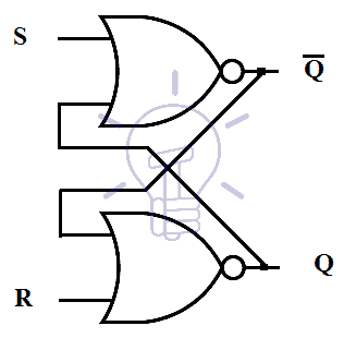
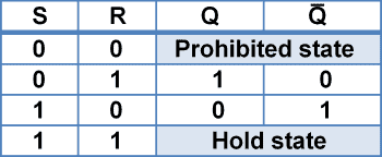
The truth table of S-R latch using NOR gates is given below:
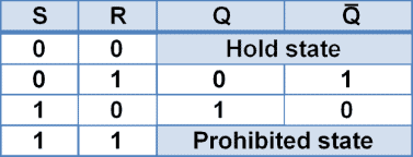
When input S = 0, R = 1, Output Q = 0, Q̅ = 1.
This input resets the output state Q to 0.
When input S = 1, R = 0, Output Q = 1, Q̅ = 0.
This input sets the output state Q to 1.
When input S = 0, R = 0, the output state remains unchanged thus it is known as “Hold state”.
When input S = 1, R = 1, the output Q & Q̅ = 0. Which violates the condition Q & Q̅ are inverse of each other, they should not be equal.
That is why this state is known as “Invalid / prohibited input state”.
S-R Latch NAND Gate
Schematic design of S-R latch using NAND is given in the figure below:
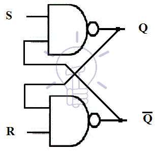
The truth table of S-R latch using NAND gate is given below:
The S-R latch using NAND gate is active low. That is why its truth table is completely opposite of S-R latch using NOR gate.
When input S = 0, R = 1, Output Q = 1, Q̅ = 0.
This input sets the output state Q to 1.
When input S = 1, R = 0, Output Q = 0, Q̅ = 1.
This input resets the output state Q to 0.
When input S = 1, R = 1, the output state remains unchanged thus it is known as “Hold state”.
When input S = 0, R = 0, the output Q & Q̅ = 0. Which violates the condition Q & Q̅ are inverse of each other, they should not be equal.
That is why this state is known as “Invalid / prohibited input state”.
Invalid or prohibited state can be avoided by converting it into any of the other 3 states.
- S-R latch set dominant
- S-R latch reset dominant
- S-R latch Hold dominant
Also read: Karnaugh Maps (K-Map), Truth Tables, Boolean Expressions & Examples
S-R Latch Set Dominant
To avoid the invalid state logic, combinational circuit is connected before S-R latch to convert the invalid input into set state;
Truth table for converting “invalid input” into “set input”
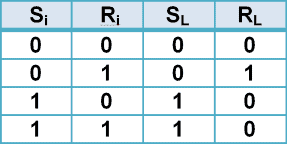
According to the truth table:
SL = Si , RL = S̅i Ri
Schematic of S-R set dominant latch is given below:
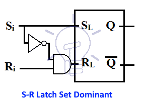
This latch sets output when invalid state input is given to it that is why it is known as set dominant.
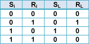
S-R Latch Reset Dominant
This latch resets upon invalid input. The invalid input is converted into reset input before feeding into the latch.
Truth table for converting “invalid input” into “reset input”
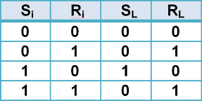
According to the truth table:
SL = SiR̅i , RL = Ri
Schematic of S-R reset dominant latch is given below:
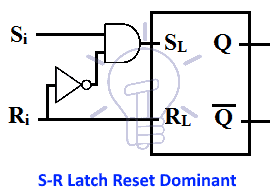
This latch resets output when invalid state input is given to it, that is why it is known as reset dominant latch.
- You may also read: Ripple Carry And Carry Look Ahead Adder
S-R Latch Hold Dominant
This latch holds its state when invalid / prohibited input is applied. The invalid input is converted into hold state input before the latch.
Truth table for converting “invalid input” into “Hold input”
According to the truth table:
SL = SiR̅i, RL = SiRi
Schematic of S-R Hold dominant latch is given below:
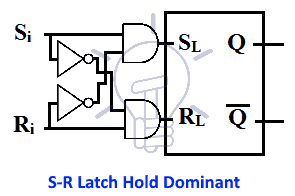
This latch holds its output state when invalid state input is applied to it, that is why it is known as hold dominant latch.
Related Articles:
- MUX – Digital Multiplexer | Types, Construction & Applications
- DEMUX – Demultiplexer | Types, Construction & Applications
Gated S-R Latch
Latch changes its state whenever input level changes but if we use a controlling signal to disable the inputs then the states won’t change. This control input is known as enable input.
Enable can be active low or active high.
“Active low enable input” allows the latch to process the input when it is low. When it is high, the input is disabled and the latch holds its state.
“Active high enable input”allow the latch to process the input when it is high and holds its state when enable input is low.
The schematic of gated S-R latches using NOR gate and NAND gate are given below.


Also read:
D-Latch
D latch stands for data latch. In S-R latch there is a restricted input condition i.e. both S, R input should not be same and either one of them should be high for set or reset. To avoid this problem, an inverter is connected with R input of S-R latch and then both inputs are combined together to form a single input D (data input).
Schematic of D-latch is given below:
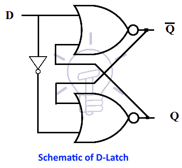
When D = 1
S = 1 & R = 0, which is “set input” so Q = 1.
And when D = 0
S = 0 & R = 1, which is “reset input” so Q = 0.
Thus in D-latch Q output follows the value of D input.
Also read:
D-Latch With Enable
D-latch also changes its state whenever input level changes. Enable pin gives the feature of enabling & disabling the input when we don’t want it to change its state.
When the input is disabled the latch retains / hold its state.
Schematics of D-latch with enable pin are given in the figure below.

Advantages & Disadvantages of Latches
Advantages:
- Latch circuits designs are more flexible as compared to flip-flop circuits.
- Digital latches are used in high speed circuit designs as they are faster and it has no need to wait for a clock input signal due to higher clock speeds as they are asynchronous in design and clock is not used over there.
- They are small and acquire less size of area as latches based circuits have small die size and they are more successful in high speed circuits designs.
- They consume less power.
- Latch is time borrowing and sharing i.e. if a circuit operation is not completed in the given time frame, they borrow the required time to execute the operation from other operational time.
- They provide aggressive clocking as compared to flip-flops based circuits.
Disadvantages:
- There is a chance to affect the race condition, hence, Latches are less predictable.
- As latches are level sensitive, there are also some chances of meta-stability.
- As they are level sensitive devices, they are complicated to analyze the latch circuits and additional CAD program should be used to test the circuit.
Application of Latches
- As latch is single bit storage element, they may be used as storage device in power gating circuits and clock
- They may be used as pulse latches where they perform the same behavior like flip-flops by pulsing the clock very quickly.
- In Asynchronous systems, D latch are used as input / output ports.
- To reduce the transit count in synchronous two phase systems, data latches may be used.
- They are widely used in data storage and computing. In short, no latches & Flip-flops, = no digital electronics and computers.
Related Articles:
Digital Logic NOT Gate – Digital Inverter Logic Gate
Digital Logic OR Gate
Digital Logic AND Gate
Exclusive-NOR (XNOR) Digital Logic Gate