What is Step Recovery Diode – SRD? Construction, Working & Applications
SRD – Step Recovery Diode: Construction, Working, Characteristics, Advantages, Disadvantages and Applications
Diodes are semiconductor-based unidirectional switches used for controlling the direction of the current. There are different types of diodes having different electrical characteristics each designed and used for their specific function. One such type of diode is the step recovery diode. It is a special purpose diode designed for its instant switching to generate sharp pulses.
What is Step Recovery Diode?
Step recovery diode (SRD) is a type of diode with very unusual doping to provide maximum switching speed at low frequency. It is also known as a voltage-dependent variable capacitor or charge storage diode. It acts like a normal diode i.e. it conducts in forward bias and blocks current in reverse bias but it instantly switches from the ON state to the OFF state. It is used to produce short pulses in various electronic circuits.
Step recovery diode has a lower doping concentration than a conventional diode. The doping concentration decreases near the junction thus the density of the charge carrier is also less around the junction. Therefore very small almost negligible amount of charge is stored near the junction. It allows very fast switching from on-state to off-state. The device snaps open, the phenomenon is called reverse snap-off. therefore, it is also known as Snap off diode.
Related Posts:
- What is Diode? Construction & Working of PN Junction Diode
- Types of Diodes and Their Applications – 24 Types of Diodes
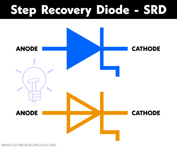
Symbol of SRD
The symbol of the step recovery diode resembles a conventional diode except for the bar is bent as shown in the figure below.
Construction
Construction-wise step recovery diode has a similar structure as a conventional diode except for its doping concentration. It is a PN junction diode with a doping concentration that decreases near the junction. The charge carrier density is maintained very low near the junction as compared to near the terminals. Due to this unusual doping, it has different switching characteristics than a normal diode. The doping profile for SRD is given below.
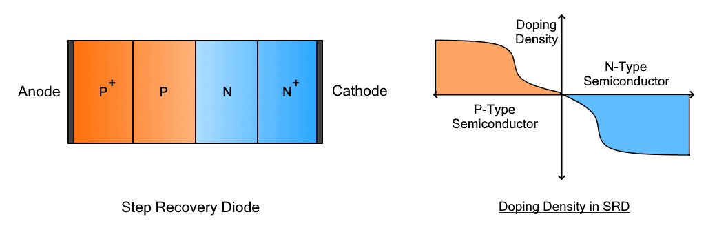
This graph shows the doping concentration throughout the structure. It decreases near the junction. The charge carriers are less near the junction. This is done to achieve fast switching due to less number of charge carriers at the junction. When a negative voltage is applied, the charge carriers in the junction take an almost half reverse cycle to drain. During that time, it conducts in the reverse direction.
Related Posts:
- Schottky Diode: Construction, Working, Advantages and Applications
- Shockley Diode: Construction, Working, Characteristics and Applications
Working
The step recovery diode works on the principle of charge storage in its junction. As we know that capacitance is formed between P-type and N-type semiconductor when combined to form a PN junction, called junction capacitance. Every diode has a junction capacitance that requires it to charge before conduction.
The junction capacitance in SRD is quite large and takes time to fully charge up in order to conduct nominal current. It operates like a normal diode in forward bias. Since it stores a huge amount of charge in forward bias, it is known as a charge storage diode. Initially, the diode exhibits very low resistance around 1 ohm which gradually increases as the stored charge increases.
Now if the applied voltage suddenly changes to reverse bias the SRD, the diode will not stop the conduction due to stored charge carriers in its junction. The stored charge carriers start conducting in the reverse direction for small duration during the negative half cycle. It takes a little time to drain the junction. The reverse current immediately stops as if the diode snaps open. Thus they are known as Snap off diodes.
If the applied frequency is increased, there isn’t enough time for the stored charge to drain. The diode conducts the negative half cycle in the reverse direction as the charged junction takes time to drain. The next positive half cycle again forward bias the diode and the junction charges up again. Thus the increase in frequency reduces the switching speed of the step recovery diode.
Characteristics of Step Recovery Diode
Here are some main features of the step recovery diode
- It instantly switches from on-state to off-state in a matter of picosecond.
- It has a very short fall time and excellent forward conductivity
- It stores a large amount of charge in forward conduction. Due to its charge storage, it’s known as a charge storage diode.
- With voltage reversal, it conducts in the reverse direction until the junction is drained of the stored charge. Then it snaps open.
- If the frequency is increased, there isn’t enough time for the charge to drain during the negative half cycle, therefore its performance decrease with frequency.
- It has unusual doping that decreases near the junction.
- It provides maximum switching speed at a low frequency
- It generates very sharp pulses.
Related Posts:
- LED – Light Emitting Diode: Construction, Working, Types & Applications
- Photodiode: Types, Construction, Operation, Modes, Performance & Applications
Advantages and Disadvantages of SRD
Advantages
Here are some advantages of step recovery diode
- It provides a very fast switching time having a very quick response for low frequency.
- It is capable of generating very short pulses in the range of mega Hz for a pulse generator.
- It can generate forward current more quickly as compared to a normal diode.
- It can double the frequency providing multiples of the input frequency.
- It has low power consumption and is very efficient.
- It has the quickest recovery time.
- It has a simple design and is inexpensive.
Disadvantages
Here are some disadvantages of step recovery diode
- Its switching speed decreases with an increase in frequency.
- It is not suitable for high-frequency applications.
Applications of Fast Recovery Diodes
Here are some applications of step recovery diode
Frequency Multiplier: SRD can be used to multiply the frequency of a signal. During its switching, it generates sharp pulses that are rich in harmonics. It is filtered to provide high-frequency signals. It can multiply a signal’s frequency up to 20 times. The SRD generates harmonics that are filtered by the band pass filter connected and provides the high-frequency multiple of the input signal.
Comb Generator: The waveform of the signal generated by a comb generator resembles the teeth of a comb. An SRD is used to generate the waveform.
Harmonic Generator: it is also used for generating different sharp pulses in a harmonic generator.
Pulse shaping: In pulse shaping, the rise and fall time of the pulse is modified to make it sharper. An SRD due to its ability to sudden snapping is able to generate very sharp pulses. Therefore it is used for pulse shaping.
Phase detector: it is used as a phase detector. It can also be used as a voltage-controlled oscillator and frequency synthesizer.
Related Posts:
- Fast Recovery Diode: Construction, Working and Applications
- Difference Between Schottky Diode and Fast Recovery Diode
- Backward Diode: Construction, Operation, Characteristics and Applications
- What is a Laser Diode? Construction, Working, Types and Applications
- Tunnel Diode: Construction, Working, Advantages, & Applications
- Zener Diode – Symbol, Construction, Circuit, Working and Applications
- Blocking Diode and Bypass Diodes in a Solar Panel Junction Box
- Diode Formulas & Equations – Zenner, Shockley & Rectifier
- Diode Symbols – Electronic and Electrical Symbols
- Applications of Diodes