Shockley Diode: Construction, Working, Characteristics and Applications
What is a Shockley Diode? Symbol, Construction, Operation Modes, Equation, VI Characteristics and Applications
Diodes are the backbone of semiconductor-based electronic devices and the breakthrough in semiconductor technology. There are different types of diodes. Shockley diode is one of the types of diode invented by American physicist William Bradford Shockley in the late 1950s. It has a similar structure as a thyristor without the gate terminal. Since it has only two terminals, it is classified as a diode.
It should not be confused with the Schottky diode that is made of MS (metal-semiconductor) junction to attain a fast switching speed.
What is Shockley Diode?
A Shockley diode is a four-layer semiconductor diode made from alternating layers of P-type and N-type semiconductor material to form a PNPN structure. It is also known as a four-layer diode or PNPN diode. It has more than one PN junction (actually three PN junctions). It conducts current in forward bias and blocks in reverse bias. The major difference between Shockley and a conventional diode is that it starts conduction once the forward voltage exceeds the break-over voltage Vbo.
Shockley diode has a similar structure as thyristor without the gate control terminal. It has two terminals which is why it is classified as a diode. It is rarely used and not easily available. however, it forms the backbone in the development of other semiconductor devices like DIAC, TRIAC and SCR, etc.
Good to know: A Shockley diode is also known as PNPN diode, hot-carrier diode or Schottky barrier diode.
Related Posts
- Schottky Diode: Construction, Working, and Applications
- Zener Diode: Symbol, Construction, Working and Applications
Symbol of Shockley Diode
The symbol of the Shockley diode resembles a conventional PN diode. But it is only half of the triangle as shown in the figure below.
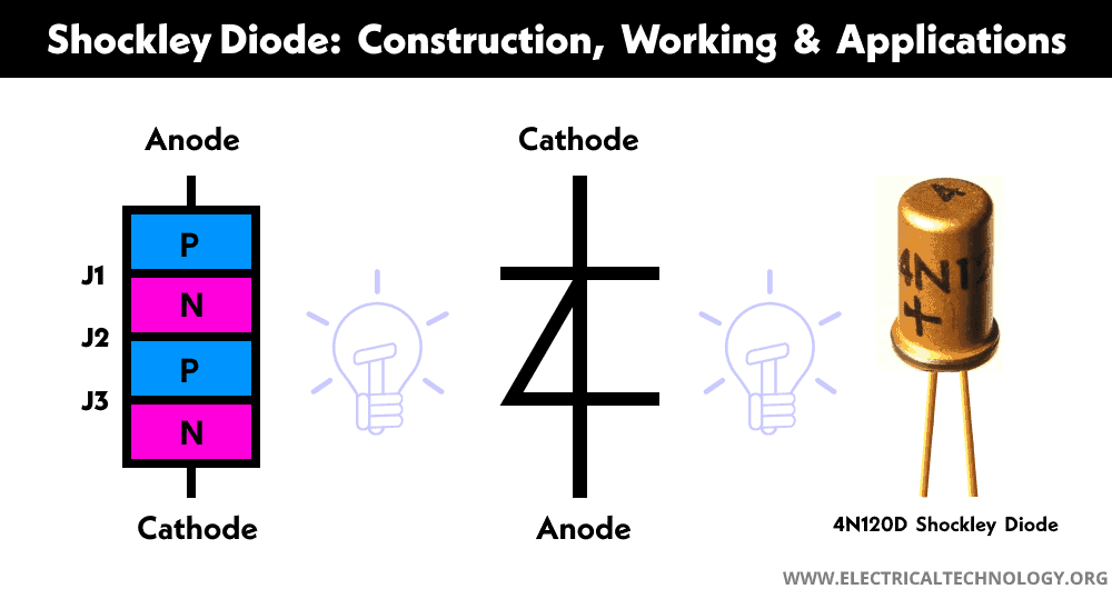
The two terminals are anode and cathode. Whereas the current flows from anode to cathode. The fig on the right shows the 4N120D Shockley diode.
Construction of Shockley Diode
It is made of four alternating layers of P-type and N-type semiconductor layers. They are sandwiched together to form a PNPN structure that resembles a thyristor. The combination of these four layers forms three PN junctions J1, J2 and J3. The anode terminal is connected to the outer P-layer while the cathode terminal is connected to the outer N-layer.

The structure of the Shockley diode can be understood using two transistor analogy. The four layers PNPN can be split into two BJT transistors (T1 PNP and T2 NPN) connected with each other. The base and the collector of both BJTs are connected together. While the emitter of PNP is the anode and the emitter of NPN is the cathode.

The junctions J1 and J3 are the base-emitter junctions of PNP and NPN respectively. While junction J2 is the combined base-collector junction of both transistors.

Its structure can also be split into the PN junction diodes D1, D2, and D3 as shown in the figure below. The diode D2 is in opposite direction to the diodes D1 and D3. The anode of D1 is Shockley anode while the cathode of D3 is Shockley cathode.
Related Posts:
- What is a Diode? Construction and Working of PN Junction Diode
- Types of Diodes and Their Applications
Working Principle of Shockley Diode
The Shockley diode can be connected in forward bias and reverse bias. In forward bias, it conducts current if the applied voltage increase above break over voltage. while in reverse bias it blocks current. These modes of operation are explained in detail below.
Forward Blocking Mode
In forward bias, the anode of the Shockley diode is connected to a higher potential than the cathode. As there are three junction J1, J2 and J3, with the application of forward bias voltage, the junction J1 and J3 becomes forward biased but the junction J2 becomes reverse biased. Due to this reverse biased junction J2, the Shockley diode does not conduct current and the applied voltage appears across the diode as if it’s blocking the current flow. However, a very small leakage current flow through it is called forward leakage current which is dependent on the temperature. This mode is called forward blocking mode.
In forward blocking mode, the Shockley diode is in OFF state offering high impedance. Therefore the diode acts as an open switch in this mode.
Forward Conduction Mode
As the applied voltage is increased, the diode leakage current slowly increases. When the voltage reaches the avalanche breakdown voltage called break over voltage or breakdown voltage or forward-peak voltage, the reverse biased junction J2 starts conduction. The resistance of the J2 junction decreases and behaves like a forward-biased junction.
The diode current rises up to a limit called holding current, the diode switch ON and the voltage across the diode starts to decrease while the current increases. This mode is called forward Conduction Mode and the Shockley diode is in ON-state.
Reverse Blocking Mode
In reverse bias, the anode of the Shockley diode is connected to a lower potential than its cathode making the anode more negative to the cathode. The junction J1 and J3 are reverse biased while the junction J2 is forward biased. This mode is called Reverse Blocking Mode. The diode is in an OFF state showing very high impedance. However, there is a very small leakage current called reverse leakage current.
If the reverse voltage exceeds the avalanche breakdown voltage of J1 and J3 called the reverse breakdown voltage, the diode breakdown, and a very large current starts flowing through it. This should be avoided at any cost to maintain the reverse voltage below the reverse breakdown Vbr limit because it permanently damages the diode.
Related Posts:
- Laser Diode: Construction, Working, Types and Applications
- Photodiode: Types, Construction, Operation Modes and Applications
How to turn off Shockley Diode?
When the Shockley diode switch ON it remains in ON state even if the applied voltage falls below the break-over voltage. It conducts current. To switch off the Shockley diode,
- The applied voltage must be reduced to zero or the diode should be reverse biased.
- The diode forward current must be reduced below the level of holding current Ih.
Shockley Diode Equation
The equation of the Shockley diode shows the relationship between the diode current and the applied voltage in both forward and reverse bias. Here is the Shockley diode equation;
I = Is (eVd/(nVt) – 1)
Where
Id = Diode current
Is = Reverse bias Saturation current
Vd = applied voltage across the Shockley diode
n = emission coefficient typically between 1 and 2 determined based on the fabrication process.
Vt = thermal voltage, it is given by
Vt = kT/q
Where
k = Boltzmann constant
T = absolute temperature in K
q = magnitude of charge
V-I characteristics of Shockley Diode
This graph represents the relation between the voltage and current through the diode. The x-axis represents applied voltage while Y-axis represents the diode current.

Reverse Characteristics
Shockley diode does not conduct current in reverse bias. Initially, there is a small reverse leakage current that depends on the thermally generated minority carriers. Thus it varies with temperature.
As the reverse voltage increases, the leakage current gradually increases until the voltage reaches the reverse breakdown voltage, Avalanche breakdown occurs and a large current starts flowing through the diode. The reverse voltage should be maintained below reverse breakdown voltage as it permanently damages the device.
Forward Characteristics
The forward characteristics show the behavior of the Shockley diode in forward bias. It is divided into the region as explained below.
Forward Blocking Region
Initially, the diode does not conduct until the voltage exceeds the breakover voltage Vbo. However, there is a small leakage current called the forward leakage current. The applied voltage appears across the diode. The device is in cut-off or off state. This mode or region is called forward blocking region.
Negative Resistance Region
When the voltage exceeds the breakover voltage Vbo, the current starts to increase while the voltage across the diode decrease showing negative resistance. Therefore this region is known as the negative resistance region. The voltage decreases until the current reaches a limit called holding current Ih. This voltage is called knee voltage Vk. However, this state remains for a very short time and the diode quickly jumps into the next region.
Saturation Region
Once the diode current reaches the holding current Ih, the voltage across the diode does not reduce further than knee voltage Vk. Whereas the current drastically increases having low voltage across the diode just like a short circuit. This region is known as the saturation region and the diode is said to be in the ON state.
Once it reaches the saturation region, the diode is latched in ON state. It does not switch off even if the voltage is reduced unless the diode current is reduced below holding current Ih. The switching-off curve is represented by the dotted line.
Related Posts:
- LED – Light Emitting Diode: Construction, Working, Types and Applications
- Tunnel Diode: Symbol, Construction, Working and Applications
Advantages and Disadvantages of Shockley Diodes
Advanatges
Here are some advantages of the Shockley diode
- It can block high reverse voltages.
- It is a latching device that maintains its state. It either stays off until voltage equal to break over voltage is applied or it stays ON until the diode current is reduced below the holding current.
- It has a low forward voltage drop
- It requires low power to switch on.
Disadvantages
Here are some disadvantages of the Shockley diode
- It has a complex structure as it is made of four layers of semiconductor material.
- To switch it OFF, the current must be decreased below the holding current by any means. Thus requiring external circuits.
- It does not have any control input or the gate input as in a thyristor.
- It is unidirectional, it conducts in only one direction as compared to a thyristor.
- It has a slow switching speed.
- Its switch ON time and switch OFF time are unsymmetrical.
- A voltage spike can switch it ON.
- Its switching can’t be controlled at high voltage.
Applications of Shockley Diodes
The Shockley diode is used for the following applications
- Triggering SCR: Shockley diode is used for triggering an SCR using the following circuit. It controls the triggering of the SCR.

When Vdc is applied, the capacitor C charges through the resistor R. When the capacitor voltage reaches the breakover voltage of the Shockley diode, the diode starts conduction and triggers or switches ON the SCR.
The SCR starts conduction and delivers power to the connected load. The SCR latches in ON state and the Shockley cannot switch it OFF. It does not switch off until its power supply is removed. The triggering time of SCR can be adjusted by varying the values of R and C in the circuit.
- Relaxation Oscillator: a relaxation oscillator is a type of nonlinear oscillator that produces a non-sinusoidal periodic waveform. They are used for generating low-frequency signals to power blinking LEDs, beepers, function generators, etc. Here is the circuit of the relaxation oscillator.
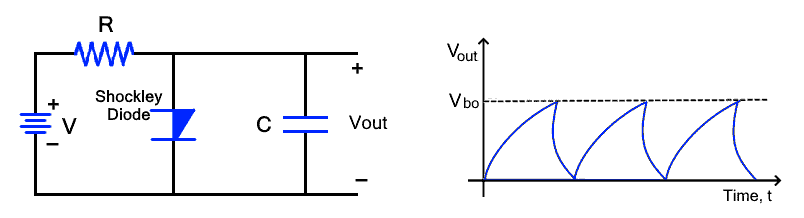
The output is taken across the capacitor C. The capacitor charges through the resistor R. Initially the diode does not conduct so the output waveform appears as the curve showing the charging of the capacitor. When the capacitor voltage reaches the diode’s break-over voltage, the diode starts conduction. The capacitor quickly discharges through the diode. The output waveform appears as a steeply decreasing curve. During discharging of the capacitor, its current drops below the holding current and the Shockley diode switch off. The capacitor starts charging again. The charging and discharging cycle continues to form a periodic waveform as shown in the figure.
Related Posts:
- Blocking Diode and Bypass Diodes in a Solar Panel Junction Box
- Difference Between Diode and Transistor
- Difference Between Diode and SCR (Thyristor)
- Difference Between Diode and Transistor
- How to Test a Diode using Digital and Analog Multimeter?
- Diode Formulas and Equations – Zenner, Shockley and Rectifier
- Diode Symbols used for different types of diodes
- Applications of Diodes
- Thyristor and Silicon Controlled Rectifier (SCR) – Thyristors Applications
- MOSFET – Working, Types, Operation, Advantages, and Applications
- IGBT: Construction, Types, Working and Applications
- GTO: Types, Construction, Working and Applications
- DIAC: Symbol, Construction, Working and Applications
- TRIAC: Symbol, Construction, Working and Applications