Schottky Diode: Construction, Working, Advantages, Disadvantages & Applications
What is a Schottky Diode? Symbols, Circuit Diagram, Construction, Working and Applications
Diodes are semiconductor based electronic components extensively used for rectification, switching, etc. It is one of the widely used electronic components. There are different types of diodes used for different applications. Schottky diode is a type of diode that is used for its high switching speed, low voltage drop, and low power consumption.
What is a Schottky Diode?
Schottky diode is a type of semiconductor diode that is formed by the junction of metal with a semiconductor. The electric current is formed only due to the majority carrier. It is also known as a hot carrier or Schottky barrier diode. It is named after German physicist named Walter H. Schottky. It has a low forward voltage drop. It is used in wave shaping, high-speed switching, RF applications, and in TTL logic gates.
A generic diode is formed by the junction between a P-type semiconductor and an N-type semiconductor. The junction formed is called the PN junction. It is formed by using silicon or germanium. While the junction is Schottky diode is called metal-semiconductor or MS junction. It is formed between metals such as Aluminum, platinum, tungsten, Chromium, gold, certain silicides, and an N-type semiconductor material.
A silicon PN junction diode has a forward voltage drop of around 0.6 to 0.7 volts while a germanium PN junction diode has a slightly lower forward voltage drop of around 0.3 to 0.4 volts. However, the practical forward voltage varies up to 0.9 volts depending on the doping level. Whereas Schottky’s forward voltage drop lies between 0.1 to 0.4 volts.
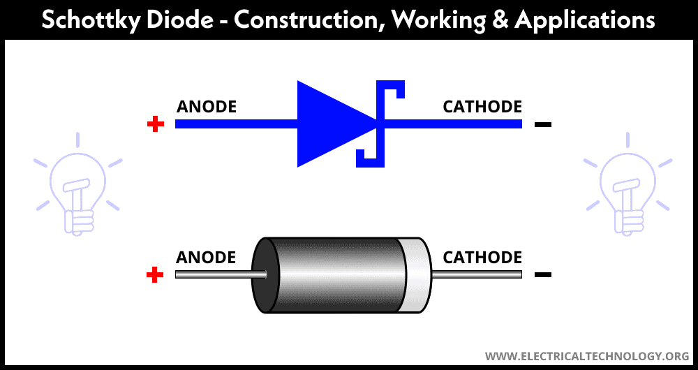
A regular diode has both semiconductor anode and cathode while the Schottky diode has a metal anode and semiconductor cathode.
Related Post: Shockley Diode: Construction, Working, Characteristics and Applications
Symbol of Schottky Diode
The symbol of the Schottky diode resembles a normal PN junction diode except the bar is modified in the shape of an “S”. Here is the symbol for the Schottky diode.
Construction
Schottky diode is constructed by forming a junction between a metal and a semiconductor called a metal-semiconductor junction or MS junction. It is a unilateral junction. The metals such as gold, platinum, aluminum, and certain silicides are used with n-type silicon semiconductors.
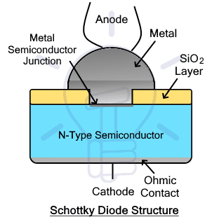 The N-type semiconductor is preferred instead of P-type because P-type semiconductor has a much lower forward voltage drop. But forward voltage drop has an inverse relation with reverse leakage current. Therefore N-type semiconductor is used with metal while forming metal semiconductor junction.
The MS junction forms a barrier called the Schottky barrier. The width of the barrier depends on the type of metal being used and the doping concentration of the semiconductor. The barrier width decreases with an increase in doping concentration. This barrier is called the potential energy barrier that prevents the flow of charge until adequate potential is applied between it. Due to high doping concentration and small depletion region, the charge carriers can easily flow through the barrier.
The Schottky diode can act as a rectifier or ohmic contact depending on the doping concentration. The rectifier Schottky diode or non-ohmic contact diode has a large width due to low doping concentration. While an ohmic contact diode has a very small barrier width due to high doping concentration. Therefore, the N-type semiconductor is lightly doped.
Related Posts:
- What is a Diode? Construction and Working of PN Junction Diode
- Types of Diodes and Their Applications
Working of Schottky Diode
Unlike PN junction diode, Schottky diode has electron as majority carrier in metal region and as well as in semiconductor region. Therefore Schottky diode does not operate like any normal PN diode. The operation of the Schottky diode is described in each phase below.
Unbiased Schottky Diode
In unbiased condition, there is no voltage source connected to the diode. There is no potential difference across the Schottky diode.

As we know that Schottky diode is made of metal and N-type semiconductor combination. The metals have free electrons but their overall charge is neutral. On the other hand, N-type semiconductor has an excess amount of free electrons thus retaining a negative charge.
The electrons from semiconductor flow through the junction into the metal during its combination. When a neutral atom accepts an electron it becomes negatively charged. On the contrary, when it lose electron it becomes positively charged. Therefore, the layer of atoms at the metal side of the junction becomes negatively charged. Consequently, a positively charged layer is formed at the semiconductor side of the junction. This layer of positive and negative charges is called the depletion region.
The depletion region forms a sort of voltage barrier for the charge carriers in the semiconductor. This barrier has a built-in potential, a threshold limit that must be crossed in order to start conduction through the junction. The built-in potential depends on the width of the barrier. Since the metal is full of free electrons, the barrier width is negligible on the metal side than on the n-type semiconductor side. Due to this small barrier, the built-in potential or built-in voltage is very small.
In order to start the conduction of charge carriers through the junction, the potential voltage applied must overcome this built-in potential. This results in the low forward voltage drop across the Schottky diode.
Related Posts
- Zener Diode: Symbol, Construction, Working and Applications
- Tunnel Diode: Symbol, Construction, Working & Applications
Forward Biased Schottky Diode
In the forward bias condition, the metal of the Schottky diode is connected with the positive terminal of the battery while the n-type semiconductor is connected to the negative terminal of the battery.
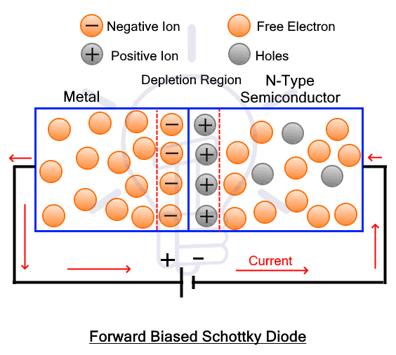
Due to the applied voltage, free electrons are generated in the semiconductor region. However, the electrons cannot pass the barrier unless the applied voltage crosses the built-in-potential limit. For most Schottky diodes, the barrier voltage is around 0.2v. when the applied voltage crosses 0.2v, the electrons get enough energy to pass the barrier. As the voltage increases, the depletion region becomes thinner and vanishes.
Reverse Biased Schottky Diode
In reverse bias condition, the negative terminal of the battery is connected with the metal of the Schottky diode and the positive terminal is connected with the n-type semiconductor. The reverse bias forms the barrier whose width increases with the increase in the reverse voltage. The reverse bias stops the current conduction but still, there is a very small leakage current. However, the leakage current can gradually rise due to an increase in reverse voltage but there is a limit. If the voltage exceeds a certain limit, the barrier permanently breakdowns and the current starts to flow in the reverse direction. This reverse breakdown permanently damages the devices.
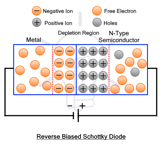
The Schottky diode has a very small recovery time as compared to PN diode because the current is only due to the majority charge carriers electrons. It quickly stops the conduction when the voltage reverses.
Related Posts:
- Laser Diode: Construction, Working, Types and Applications
- Photodiode: Types, Construction, Operation Modes & Applications
IV Characteristics of Schottky Diode
The I-V or current-voltage characteristics of a device show the relationship between the voltage and the current flowing through the device. Here is the IV characteristic curve of a Schottky diode in comparison with PN junction diode. The horizontal line shows the voltage across the Schottky diode while the vertical line shows the current through the device.
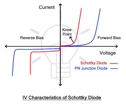
As you can see, the IV curve for both Schottky and PN diode is similar except for the knee voltage. The knee voltage or turn ON voltage for the Schottky diode is very low as compared to PN diode. Due to this the forward voltage drop is very low and the power dissipation across the diode becomes very low.
According to the curve, the Schottky diode does not conduct until the voltage reaches the knee point. However, there is still a small leakage current called forward leakage current. Above the knee point which is around 0.2 – 0.4 volts for most Schottky diodes, the current increases exponentially.
In reverse bias, there is no current flow except the reverse leakage current that is shown in the third quadrant of the graph. The reverse leakage current increases very slowly and almost negligibly with an increase in reverse voltage until the reverse breakdown. At this point, the device starts conducting in the reverse direction and is permanently damaged. Comparatively, the reverse leakage is higher and the reverse breakdown voltage is lower than PN diode due to the low forward voltage of the Schottky diode.
Related Posts:
- PNP Transistor – Construction, Working and Applications
- NPN Transistor – Construction, Working and Applications
Advantages and Disadvantages of Schottky Diode
Advantage
Here are some advantages of the Schottky diode.
- It has a very low forward voltage drop or low turn-on time.
- It has very low power dissipation across it.
- It has a very fast recovery time.
- It has a high switching speed.
- It can operate at a very high frequency.
- Its efficiency is higher as compared to PN junction diode.
- Due to the small depletion region, the junction capacitance is also low.
- On the contrary, the current density is high due to the small depletion region.
- It operates quietly as compared to PN diode.
Disadvantage
Here are some disadvantages of Schottky diode.
- Due to the low forward voltage drop, the Schottky diode has a higher reverse leakage current as compared to PN junction diode.
- It has a lower reverse breakdown voltage. Therefore it cannot handle large reverse voltages.
- It has a comparatively low reverse voltage rating.
- It has a large reverse saturation current.
Related Posts:
- Bipolar Junction Transistor (BJT) | Construction, Working, Types and Applications
- Types of Transistors – BJT, FET, JFET, MOSFET, IGBT and Special Transistors
Applications of Schottky Diode
Schottky diode just PN diode is used for switching and especially for its low losses and high speed. Here are some applications of the Schottky diode.
- It is used in high-speed high-power rectifiers.
- It is used in RF (radio frequency) high-frequency applications. Such as RF mixer and detector.
- It is used as a signal detector in the FM demodulator circuit.
- Due to low losses and high switching speed, it is used in TTL logic circuits in digital devices.
- It is used in voltage clampers circuits.
- Due to its low forward voltage, it is used in photovoltaic systems (solar cells) to prevent reverse current from the batteries or load connected.
- It is used in SMPs (switched-mode power supplies)
- It is used for loads that require more than one battery. It is used to prevent the flow of current in between the batteries that can damage them.
Related Posts:
- LED – Light Emitting Diode: Construction, Working, Types & Applications
- Blocking Diode and Bypass Diodes in a Solar Panel Junction Box
- Difference Between Diode and Transistor
- Difference Between Diode and SCR (Thyristor)
- Difference Between Diode and Transistor
- How to Test a Diode using Digital & Analog Multimeter?
- Diode Formulas & Equations – Zenner, Shockley & Rectifier
- Diode Symbols used for different types of diodes
- Applications of Diodes
- Thyristor and Silicon Controlled Rectifier (SCR) – Thyristors Applications
- MOSFET – Working, Types, Operation, Advantages, and Applications
- IGBT: Construction, Types, Working and Applications
- GTO: Types, Construction, Working and Applications
- DIAC: Symbol, Construction, Working and Applications
- TRIAC: Symbol, Construction, Working and Applications


On one diagram you have the anode marked with a “+” and on another diagram it is marked with a “-“
Can you please show me that diagram ?