Photodiode: Types, Construction, Operation, Modes, Performance & Applications
What is a Photodiode? Symbol, Circuit, Construction, Types, Working, Characteristics, Modes, Performance and Applications
A photodiode is a type of semiconductor-based photosensor or light sensor that is used to detect and measure the intensity of light. It is used in the light-based application and use light to control various other electrical devices. This article covers all the basics of photodiode and its various types in detail.
What is Photodiode
A photodiode is a type of diode that converts light energy into electrical energy. It is essentially a light sensor that generates an electric current when light falls on it. It is also known as a light detector, light sensor, or photo sensor. The phenomenon through which the light energy is converted into electrical energy is called the photovoltaic effect. A solar cell or solar panel consists of an array of photodiodes also called photovoltaic cells that convert solar energy into electrical current.
It is a semiconductor device made from a PN junction. A P-type semiconductor and an N-type semiconductor material is joined together with an additional Intrinsic layer between them. It is designed to operate in reverse bias conditions i.e. the P side of the photodiode is connected to the negative while the N side is connected to the positive terminal of the battery.

The material used to manufacture photodiodes are but are not limited to silicon, germanium, indium gallium arsenide. The type of material and the doping concentration determines the performance parameters of photodiode such as response time, sensitivity, breakdown voltage, dark current and cost benefits.
It has a highly sensitive junction or in some cases the intrinsic region that generates electron-hole pair when light struck on it. The junction is exposed using a window lens for the incident light. The electric current is generated that is proportional to the intensity of the light falling on it. This phenomenon is called the photovoltaic effect.
Related Posts:
- What is the Difference Between Photodiode and Phototransistor?
- What is the Difference between LED and Photodiode?
- LED – Light Emitting Diode: Construction, Working, Types, & Applications
Symbol of Photodiode
The symbol of a photodiode is exactly like an LED light-emitting diode with rays of light falling on it as shown in the figure below.
 It has two terminals anode and cathode. The anode is the longer terminal while the cathode is the shorter terminal.
- Related Post: Different Types of Diodes Symbols
Construction
A typical photodiode is made from two layers of P-type and N-type semiconductor joined together to form a PN junction. As it is a light sensor, the junction is exposed for light rays by covering it with a glass or optical lens. The lens increases the surface area to collect more light and increase its intensity. The remaining portion of the photodiode is covered in a black layer or metalized. The structure of a photodiode is given below.

The given figure shows the cross-sectional structure of a typical PN photodiode. It is made from the joining of two layers P and N. The P-type material is lightly doped while the N-type material is heavily doped. The joining of these two layers forms a region due to the movement of (+) ions from P-type material and the movement of (-) ions from N-type material. This region is free of any charge carriers. However, there is an electric field across this depletion region. This electric field is responsible for the flow of current in only one direction when an electron-hole pair is generated. It is why photodiodes are reverse biased or not biased at all. Forward biasing may damage the photodiode permanently. The P+ active region is covered with an anti-reflective AR layer or glass while the remaining body is metalized or painted black. Metal contacts are used for cathode and anode.
The front side of the diode can be classified into active and non-active regions. The active region as it name suggest is the area where the light energy is converted into electrical energy, therefore, it is covered with anti-reflective material to absorb maximum light falling on it. The non-active area is covered with SiO2 layer.
Working of a Photodiode
A PN photodiode is similar to a conventional PN junction diode. When a PN junction diode is reverse biased, the depletion region widens. Minority charge carriers are generated that constitute the reverse current of the diode. This reverse current is directly proportional to the applied reverse voltage.

Similarly, in the photodiode, there is a built-in-potential difference across the depletion region. When a light ray or photon of enough energy (hv) greater than the energy gap (Eg) falls on the junction of the photodiode, it dislodges or removes an electron from its valance band into the conduction band. The electron lefts an empty space called a hole, thus electron-hole pair is generated. This phenomenon is also called the inner photovoltaic effect. Under the influence of an inbuilt electric field, the electron and hole moves in opposite directions i.e. the electron moves toward the cathode and the hole moves toward the anode. This current is called photocurrent and it is directly proportional to the intensity of the falling light.
In photodiodes, there is still a flow of current even when there is no light source or photons falling onto its junction. This current is known as dark current. It is extremely small in microampere. It resembles the leakage current of any conventional PN junction diode. It is the unwanted current in reverse bias that varies directly with temperature and it must be reduced to have increased sensitivity of the photodiode. The total current of any photodiode is the sum of the photocurrent and the dark current.
Related Posts:
- Zener Diode – Symbol, Construction, Circuit, Working and Applications
- Tunnel Diode: Construction, Working, Advantages, and Applications
Modes of Photodiode
A photodiode can operate in the following three modes.
- Photovoltaic Mode
- Photoconductive Mode
- Avalanche Diode Mode
Photovoltaic Mode
This mode is also known as Zero Bias Mode as there is no biasing or external voltage source connected to the photodiode. When light or photon hits the depletion region, electron-hole pair is generated that moves in opposite direction away from the junction under the influence of the inbuilt electric field. As a result, a current is generated if it is connected in a closed circuit or a potential difference is generated between the cathode and anode if it is an open circuit.

In the case of an open circuit, a forward voltage proportional to the light intensity falling on the active region is generated across its anode and cathode. This voltage is in forward bias mode as the potential at the anode is greater than the cathode.
 In the case of a closed circuit, a forward current flows through the circuit. This forward current is equal to the sum of photocurrent and dark current. This phenomenon is known as the photovoltaic effect and it is mainly responsible for the operation of solar cells.
Photovoltaic mode provides low-level current variation (low dynamic range) with nonlinear voltage. It is used in low-level frequency applications and low-level light. This mode has low electronic noise. But it has a slow response time due to maximum junction capacitance due to an unbiased system.
Photoconductive Mode
In photoconductive mode, the photodiode is reverse biased i.e. its anode is connected with the negative terminal and the cathode is connected with the positive terminal of the battery or the cathode is at higher potential with respect to the anode. Therefore this mode is also known as a reverse-biased mode.
 Due to reverse bias, the depletion region expands and varies directly with the increase in reverse voltage. Due to the large area, more charge carriers are collected more quickly from the junction. It also reduces the capacitance of the junction resulting in a much quicker response time.
In photoconductive mode, apart from the photocurrent, there is another current called dark current in the reverse direction. Dark current is due to the reverse bias in the absence of light. It greatly depends on the temperature and varies directly with it. It also depends on the type of material and the active region of the photodiode. It is an unwanted current that generates electrical noise.
Related Posts:
- Zener Diode and Zener Voltage Regulator Calculator
- Simple Overvoltage Protection Circuit using Zener Diode
Avalanche Mode
In avalanche mode, the photodiode is connected with high reverse bias voltage. The high reverse voltage increases the depletion width and the potential across it. Due to high potential, the electron-hole pair flows with maximum speed hitting more atoms in its path resulting in more photocurrent. Therefore, avalanche mode has high internal gain and responsivity.
Photodiode Circuit
When the photodiode is used in an external circuit, it is mostly used in reverse biased conditions. The anode is connected with the negative or ground and the cathode of the photodiode is connected with the positive terminal of the battery as shown in the figure below.
 Photodiode cannot power any electronic device as the current generated by itself is extremely small. Therefore, a power source is used to increase the current supplied to the load.
Quantum Efficiency of Photodiode
Quantum efficiency is the fraction of incident photons that are absorbed by the photodiode and generate electrons. In other words, the quantum efficiency is defined as the fraction of incident photon that contributes to the photocurrent. It is directly proportional to the responsivity.
The quantum efficiency can be maximized by reducing the reflection using anti-reflection coating. It highly depends on the wavelength of the incident light. The quantum efficiency can be very high up to 95%.
Related Posts:
- Bipolar Junction Transistor (BJT) | Construction, Working, Types and Applications
- Types of Transistors – BJT, FET, JFET, MOSFET, IGBT and Special Transistors
Performance Parameters
The performance of photodiode depends mainly on the following parameters.
Response Time
Response time for a photodiode can be defined as the time a charge carrier takes to cross the junction. It greatly depends on the capacitance of the junction. Whereas the junction capacitance depends on the width of the junction. Larger the junction’s width, the smaller the capacitance and lower the response time. To provide a better performance, response time is kept minimum.
Responsivity
Responsivity is the ratio of the photocurrent generated from the incident light to the actual power of the incident light. The unit of responsivity is A/W (current/power). Responsivity is kept higher to offer better performance.
Dark Current
Dark current is the current in the photodiode in reverse bias when there is no light. It is similar to the reverse leakage current in a conventional PN junction diode. It is very small often measured in microamperes. However, it is minimum in unbiased or zero bias mode. It varies directly with the change in temperature. Dark current causes electronic noise in the system. Therefore it is kept minimum to offer better performance.
Breakdown Voltage
The breakdown voltage is the maximum reverse voltage a photodiode can tolerate. If the applied voltage crosses the breakdown voltage, the reverse leakage current or dark current will increase exponentially and the diode will get permanently damaged. Photodiodes must be operated below this level. The breakdown voltage decreases with an increase in temperature.
Related Posts:
- PNP Transistor – Construction, Working and Applications
- NPN Transistor – Construction, Working and Applications
VI Characteristics of Photodiode
The VI characteristics curve shows the relationship between the voltage and current of a device. The horizontal axis or x-axis represents the voltage while the vertical axis or y-axis represents the current through the device. Given below is the characteristic curve for the photodiode.

As we know that photodiode operates in reverse bias, therefore the graph is between the reverse voltage and the reverse current. The reverse voltage is represented on the negative x-axis while the reverse current is represented in microamperes on the negative y-axis.
The reverse current does not vary with a change in the reverse voltage. However the reverse current increases with an increase in the intensity of the incident light. At zero light intensity or no light, there is no significant reverse current except for a very small constant current called the dark current. By increasing the intensity of light the reverse current increases linearly
Types of Photodiode
There are many different types of photodiodes available. They all operate on the same basic principle. Each one of them is specifically designed to have at least one enhanced parameter such as high speed, low noise, high efficiency, etc. Here are a few of the most used photodiodes
PN Photodiode
PN photodiode is the first type of photodiode developed. It has a single PN junction just like any conventional diode. It has a small depletion region that can be expanded by applying reverse voltage. Since the junction width determines the junction capacitance, increasing the width will decrease the capacitance but the reverse bias also increases the flow of unwanted current called the dark current. It creates electrical noise in the system. It is smaller in size with lower response time and sensitivity. They are not been widely used since the development of PIN photodiode.
PIN Photodiode
PIN or P-I-N photodiode is a type of photodiode that is essentially a modified, more efficient form of PN photodiode. It is developed by inserting an Intrinsic semiconductor material between the P-type and N-type material. The intrinsic material is a highly resistive material that improves its performance such as speed, current and efficiency.
Structure
It is made of three layers P-type, N-type and intrinsic semiconductor material. The intrinsic layer is sandwiched between the P-type and N-type layer to form two junctions P-I and I-N as shown below.

The intrinsic semiconductor is the pure form of semiconductor that has an equal amount of electrons and holes. Therefore, there are no charge carriers in an intrinsic semiconductor. While a P-type and N-type semiconductor is formed by adding different impurities in the intrinsic material. P-type semiconductor has holes as majority charge carriers while N-type semiconductor has electrons as majority charge carriers.
Working
The intrinsic layer increases the depletion area. It further increases with the application of reverse voltage. The P-layer is connected with the negative terminal and the N-layer is connected with the positive terminal of the voltage source. The majority charge carriers in the p layer and n layer are pulled in opposite directions. The depletion width increases with an increase in reverse voltage until it is equal to the intrinsic layer. At this moment the intrinsic layer is free of any free charge carriers.
Since the depletion region became wider, most of the incident light or photons are utilized and generate huge number of electron-hole pairs. The electrons generated in the intrinsic region moves toward the P layer and the holes move towards the N layer enabling the flow of electric current.
The intrinsic layer has many benefits. It increases the width of the depletion region. It increases the active region or the area on which light falls, therefore, it increases the efficiency. The large depletion region allows more electron-hole pair generation resulting in more photocurrent. It also reduces the junction capacitance that increases the speed of the photodiode. But it requires high reverse bias voltage that also creates electrical noise in the system.
Advantages
- Its efficiency is higher than the PN photodiode.
- Its response time is faster than the PN photodiode.
- It is suitable for high-frequency applications in electronic circuits.
- It is more sensitive as compared to PN photodiode.
- It has larger bandwidth.
Related Post: Tunnel Diode: Construction, Working, Advantages, and Applications
Avalanche Photodiode
Avalanche Photodiode is another type of photodiode diode that has a similar working principle but it provides high current gain thanks to impact ionization. Impact ionization is the phenomenon when a charge carrier with sufficient kinetic energy collides with other atoms and removes the electrons creating more charge carriers. This is also known as the avalanche effect. Avalanche Photodiode is very sensitive having a high current gain. Therefore, they are used for low-light applications. However, it requires high reverse voltage and creates excess electrical noise.
Structure
The structure of Avalanche photodiode resembles PIN photodiode. It is made of four layers i.e. P, I, P and N layers as shown in the figure. The two layers P+ and N+ at the end terminal are heavily doped which forms anode and cathode respectively. While the intrinsic I layer and the P layer is lightly doped.
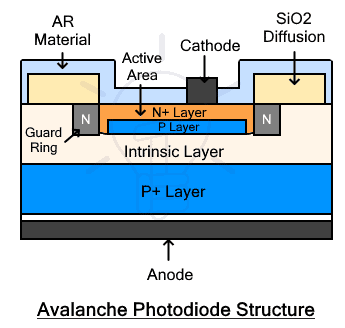
Its construction is complicated as compared to PIN photodiode due to the guard ring and uniform junction. The guard ring helps protect the photodiode from edge breakdown. The N layer is the thinnest layer. The depletion width is thinner as compared to the PIN photodiode.
Working
Avalanche photodiode operates at very high reverse bias voltage. It develops a strong electric field across the depletion region. When light or photon strikes the photodiode, it generates electron-hole pair. This electron and hole moves toward P+ and N+ region at a very high speed due to the strong electric field. Due to the high kinetic energy of the electron, it collides with other atoms in the material and knocks off electrons creating more electron-hole pairs.it is called impact ionization. Similarly, these electrons accelerate again and collide with other atoms releasing further electrons resulting in exponential growth of charge carriers. It is known as Avalanche multiplication. Therefore Avalanche photodiode generates a higher photocurrent than PIN photodiode.
The high reverse voltage increases its sensitivity and response speed but it also makes it more susceptible to electrical noise. Dark current also increases with reverse voltage. The noise depends on temperature. Therefore large heat sinks are used with it.
Advantages
- It can sense low-intensity light
- It has very high sensitivity.
- It provides a high level of signal gain.
- It provides greater SNR (Signal to Noise) ratio
- It has s very fast response time.
Schottky Photodiode
Schottky Photodiode is another type of photodiode made from a combination of metal and semiconductor. Therefore it is also known as a metal-semiconductor or MS junction diode. Unlike PIN and avalanche photodiode, it does not contain any PN junctions. It operates similar to any other photodiode. It enables the Schottky photodiode to have high speed and especially long wavelength detection.

The MS junction operates similar to the intrinsic layer. The metal usually gold (Au) is utilized to form a transparent metallic layer over the N-type semiconductor layer. The photons pass through the gold layer and absorb in the N-type layer. The photon releases an electron-hole pair in the depletion region that is swept away by the built-in electric field.
The response time of the Schottky photodiode depends on the doping concentration of the N-type semiconductor. Adjusting the doping concentration varies the width of the depletion region. The advantage of the Schottky photodiode over other photodiodes is that it makes only one metal-semiconductor connection when it is connected to an external circuit. Therefore, it does not require ohmic contacts. Due to the absence of a P-type semiconductor, it has a quite faster response. It enables it to operate at a very short wavelength and frequency of up to 50 Ghz.
- Related Posts: Types of Diodes and Their Applications – 24 Types of Diodes
Advantages and Disadvantages of Photodiode
Advantages
Here are some advantages of Photodiode
- It operates on light energy.
- It facilitates fast communication through an optical fiber.
- It creates very low noise.
- It generates a low dark current as compared to the phototransistor.
- It has high quantum efficiency.
- It has very low resistance.
- It is rugged and has a longer lifespan
- It operates on low voltage.
- It has a linear response
- It is cost-effective.
Disadvantages
Here are some disadvantages of Photodiode
- The active area is relatively small.
- It has lower sensitivity than other components.
- It requires an external power source to supply sufficient current to a load.
- It requires amplification when operated under low light intensity.
- The simple PN photodiode has a high response time.
- Thermal noise greatly affects its performance.
- It has poor temperature stability.
- It uses offset voltage.
Related Post: Applications of Diodes
Applications of Photodiode
Photodiodes are basically used to detect and measure light intensity, therefore it has numerous applications in almost every field. Here are some applications of Photodiode
Electrical Isolation:
Photodiodes are used in opt couplers to electrically isolate two circuits. It isolates any low voltage sensitive circuit from a high voltage circuit. The circuits are optically coupled and electrically isolated.
Renewable Energy:
Photodiodes are extensively used to convert solar energy into electrical energy to power our daily use equipment. They are used at the domestic as well as industrial level. Hundreds of panels each containing arrays of photodiodes are used in a single solar plant to produce electrical energy.
Optical Communication:
High-speed photodiodes such as PIN photodiodes are used for high-speed optical communication using fiber optic cables.
Building Safety:
It is also used in fire and smoke alarms to prevent any kind of fire hazard in a building. Its light sensor can detect smoke.
Medical Instruments:
Photodiodes also find multiple applications in medical Instruments such as CT scans, PET scanners, sample analyzers, etc.
Burglar alarm
In a burglar alarm, there is a light source fixated in such a way that it constantly strikes the photodiode and generates a constant current. If something or someone passes through and causes obstruction to the light, the diode current falls and triggers the alarm.
Counter
The photodiode can be used to count objects that pass between it and a continuous source of light.
- It is used as a photo sensor to measure different levels of light intensity in a digital camera.
- It is used to detect visible as well as invisible (IR) light.
- It is used as an optical encoder and decoder.
- It is used as a position sensor, proximity sensor and bar code reader.
- It is used in automatic street light that switches according to the light falling on it.
- It is used in infrared remote to control any device remotely such as a TV, air conditioner, etc.
- It is used in a compact disc CD player, scanner,
- It is used in printers to detect and count pages.
- It is used as a variable resistance device whose resistance varies with light intensity.
- It is used in digital logic circuits due to its high speed and low voltage requirement.
- They are used in character recognition techniques.
Related Posts:
- Diode Formulas and Equations – Zenner, Schockley and Rectifier
- How to Test a Diode using Digital and Analog Multimeter? – 4 Ways.
- Blocking Diode and Bypass Diodes in a Solar Panel Junction Box
- Simple Overvoltage Protection Circuit using Zener Diode
- Thyristor and Silicon Controlled Rectifier (SCR) – Thyristors Applications
- MOSFET – Working, Types, Operation, Advantages, and Applications
- IGBT? Construction, Types, Working and Applications
- GTO? Types, Construction, Working and Applications
- DIAC? Symbol, Construction, Working and Applications
- TRIAC? Symbol, Construction, Working and Applications
- Difference Between Diode and SCR (Thyristor)
- Difference Between Diode and Transistor