Tunnel Diode: Construction, Working, Advantages, & Applications
What is a Tunnel Diode? Symbols, Construction, Operation, Characteristics and Applications
A diode is the most fundamental component used in electronic circuits. However, there are different types of diodes being used each designed for its specific applications. One such for we are going to discuss here in this article is Tunnel Diode.
A Japanese physicist Leo Esaki in 1957 invented a new type of diode by increasing the doping concentration of a PN junction diode. In doing so, he observed “Negative Resistance” due to the “Quantum mechanical effect” which he named the “Electron Tunneling” effect. He was awarded the Nobel prize for discovering the electron tunneling effect.
Therefore the Diode was named Tunnel Diode or Esaki Diode. It has negative resistance which means the current decreases with an increase in voltage in its operating range. It has the capability of high-speed switching thus it is used in high-frequency applications.
What is Tunnel Diode?
A Tunnel diode also known as Esaki diode is a type of diode made from the PN junction of a heavily doped semiconductor whose current decrease with an increase in voltage due to negative resistance. This phenomenon is also called electron tunneling. It enables high-speed switching that makes it suitable for high-frequency applications such as in computers.
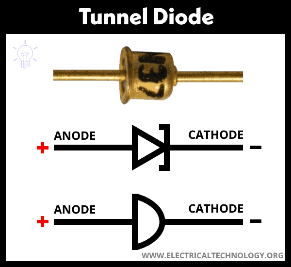
Symbol of Tunnel Diode
The Tunnel diode can be represented using two different symbols add shown in the figure below.

It had two terminals named anode and cathode. The anode is the P-region while the cathode is the N-region. The anode is positively charged with holes in the majority and it attracts electrons from the cathode. While the cathode is negatively charged with the majority of electrons and attracts holes from the anode.
- Related Post: Different Types of Diodes Symbols
Construction
During the construction of the Tunnel diode, the following two factors are really important.
- Material (peak current to valley current ratio)
- Doping Concentration
Material plays a vital role in the performance of the tunnel diode. When a forward voltage is applied, the current increases up to peak current as in any other normal diode. With a further increase in the forward voltage, the current starts decreasing down to the minimum point called the valley point.
The ratio of peak current to valley current must be large to enable electron tunneling. Silicon has a very small ratio of peak current to valley current compared to germanium. Therefore, silicon is not suitable for tunnel diodes. Materials such as germanium, gallium arsenide, and gallium antimonide are used for the construction of Tunnel diode
The semiconductor used for tunnel diode must have a very high doping concentration. Semiconductors are naturally neutral i.e. the number of electrons and holes are equal. Impurities are added to increase the number of electrons or holes to form either n-type or p-type semiconductors.
The doping level is almost 1000 times greater than any normal diode. The heavy doping reduces the width of the depletion region. This also reduces the reverse breakdown voltage of the diode.
Here is the structure of the Tunnel diode given below.

As far as the construction of a Tunnel diode is concerned, it is very simple to fabricate. The whole structure is hermetically sealed with a ceramic body. A very small tin dot of 50 μm in diameter is alloyed to a square pallet of 0.5 mm that is made of heavily doped n-type Ga, GaAs, or GaSb.
The pallet is then soldered on top of the anode. The anode also helps in heat dissipation. The tin dot is connected to the cathode through a mesh screen that helps in the reduction of inductance.
Electron Tunneling
Electron tunneling of quantum tunneling is a quantum effect where charge carriers or electrons easily move through a junction due to its very small depletion region. An electron must acquire a certain potential higher than the in-built potential of the barrier to pass through it.
Since the depletion region in the tunnel diode is largely reduced in nanometers thanks to heavy doping concentration, the electrons can punch through the junction even if the voltage is lower than the barrier potential. This effect is called electron tunneling & the diode is called the tunnel diode.

We can compare a conventional diode with a tunnel diode using the given figure. The combination of p & n semiconductors forms a junction called the barrier or depletion region. It is made of an equal number of+ve & -ve ions. Therefore it has no majority carriers.
Due to the combination of P & N semiconductors, a potential is formed across the barrier called the barrier potential. The electron must acquire energy greater than the barrier potential to pass through it. However, quantum mechanics say that if the depletion width becomes very small the electrons can penetrate through the barrier having lower energy.
The barrier potential is directly proportional to the junction width. The tunnel diode has a very small barrier width in nanometers as compared to a normal PN diode.
Therefore the electrons in a normal diode require applied voltage greater than the barrier potential to pass through. While tunnel diode can conduct a large current at a small applied voltage lower than the barrier potential due to electron tunneling from the conduction band of the n-region into the valance band of the p-region.

Electron Tunneling can be clarified using the given energy bands. In a tunnel diode, The conduction band and valance band energy level of an n-type semiconductor is lower than the energy level of conduction and valance band of a p-type semiconductor.
Therefore the conduction band of n-type (that carries electrons) & the valance band of p-type (holes) fall at the same energy level. So the electrons from the conduction band of the n-region pass through the narrow junction into the valence band of the p-region.
Due to electron tunneling, the tunnel can conduct a large current at a small forward voltage
- Related Posts: Types of Diodes and Their Applications – 24 Types of Diodes
Working of Tunnel Diode
The working of the Tunnel diode is explained in each separate condition.
Unbiased Condition
In unbiased conditions, there is no voltage applied to the tunnel diode. In unbiased conditions, the conduction band of a p-type semiconductor overlaps the valance band of an n-type semiconductor due to heavy doping. Therefore the electrons from the n-region fall nearly at the same energy level as the holes from the p-region.
Due to similar energy levels & increase in temperature, the electrons from the n-region tunnel into the p-region. While the holes from the p-region tunnel into the n-region.

However, there is no current flow through the tunnel diode in unbiased conditions because the net current is zero due to the tunneling of the number of electrons and holes are equal.
Forward Biased
In forward biased condition, the p-side is connected to the positive terminal and the n-side is connected to the negative terminal of the battery. The output characteristics of the Tunnel diode vary with an increase in applied forward voltage.
Initially, it acts as a normal diode whose current increase with an increase in voltage. After a certain voltage level, the current starts decreasing known as the negative resistance. Each level of the stage is explained below.
Small Voltage Applied
When a small forward voltage whose magnitude is less than the built-in barrier potential is applied to the tunnel diode, no electron is passed through the depletion region & no forward current is generated due to it. The small applied potential reduces the energy band gap between the electrons & holes and they start to overlap with each other as shown in the figure.
The energy level of the electrons in the conduction band & holes in the valance band becomes slightly similar.

Due to the overlapping of energy bands & the thin depletion region, a small number of electrons tunnel through the depletion region using the tunneling effect. This electron tunneling causes a small forward current through the diode.
Applied Voltage Slightly Increased
When the applied voltage is increased, the electrons are energized and the energy band gap reduces even further. In fact, the energy level of the electrons in the conduction band and the holes in the valance band become parallel i.e. both are at the same level as shown in the figure. Therefore, the electrons can easily pass through the depletion region into the p-region.
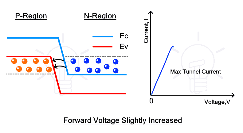
In such conditions, the forward current reaches its highest peak. This large forward current is the product of two factors; flow of energized electrons & flow of electrons due to the thin depletion region.
Applied Voltage Further Increased
When the applied voltage is further increased, the conduction band and the valence band start to misalign and the energy band gap starts to increase. Due to this misalignment, the forward current starts to decrease down to the minimum point called the valley point. This is called negative resistance & the tunnel diode is designed to operate in this region.

Increasing the voltage further completely diminishes the overlapping between the conduction band of the n-region and the valence band of the p-region. In this condition, there is no tunnel current as the energy band gap is huge. However, there is a large forward current due to the high potential applied between the thin depletion region. Therefore, the diode starts to operate as a normal PN Junction diode.

Related Posts:
- Zener Diode – Symbol, Construction, Circuit, Working and Applications
- Schottky Diode: Symbol, Construction, Working and Applications
Reverse Bias
In the reverse bias condition, the p-side is connected to the negative terminal & the n-side is connected to the positive terminal of the battery. In such conditions, the tunnel diode operates as a back or backward diode.
Since it has a very thin virtually no depletion region due to the heavy doping concentration, it can conduct a large amount of reverse current. It remains in a state of conduction in reverse bias as in backward diode.
Due to heavy doping concentration, the peak inverse voltage PIV is small as compared to the maximum forward voltage.
Equivalent Circuit of Tunnel Diode
A Tunnel Diode can be represented by an equivalent circuit using a resistor, inductor & capacitor as shown below. The main feature of the Tunnel diode is the negative resistance region & the diode resistance in this region is represented by -Ro. The Co represents the capacitance of the junction. The Ls is the series inductance due to the leads of the diode & Rs is the series equivalent resistance.

Related Posts: Photodiode: Types, Construction, Operation, Modes, Performance & Applications
VI Characteristics of Tunnel Diode
The VI Characteristics show the relationship between the applied voltage and the diode current as shown below. The applied voltage V is represented by the x-axis and the diode current I is represented by the y-axis. The graph shows the operation in both forward and reverse bias
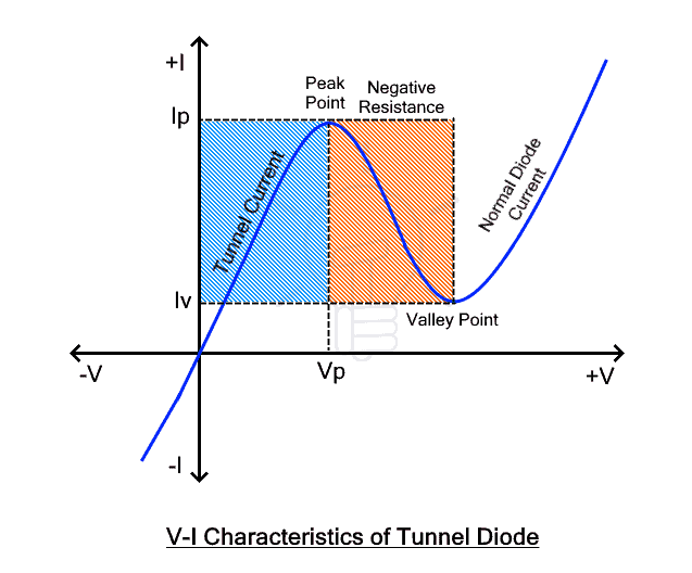
In forward bias, initially, there is no forward current at zero voltage. However, with the increase in voltage, the diode immediately starts conduction & the forward current increases up to the peak current Ip, at this point the voltage is Vp.
With a further increase in voltage above Vp, the forward current decreases down to the minimum value Iv called valley point & this minimum current is called valley current. This region is called the negative resistance region. The Tunnel diode does not consume power but rather produces it in this region & it mainly operates in this region.
Beyond the valley point, the diode operates like any conventional diode. The forward current increase with an increase in voltage.
In reverse bias, the diode conducts a large reverse current due to heavy doping concentration. It has a very small almost zero depletion width. Similarly, It operates like an excellent conductor in reverse bias. Moreover, It is only operated in forward bias.
Related Posts:
- Bipolar Junction Transistor (BJT) | Construction, Working, Types and Applications
- Types of Transistors – BJT, FET, JFET, MOSFET, IGBT and Special Transistors
Advantages & Disadvantages of Tunnel Diode
Advantages
Here are some of the advantages of Tunnel diode
- A tunnel diode has negative resistance that is useful in oscillators and amplifiers.
- It operates at a very high switching speed
- It is suitable for high frequency
- It is easy to operate.
- It has low power dissipation and is energy efficient.
- It has a high disability with a longer life span.
- It operates very smoothly with low noise and it is also immune to noise interference.
- It has a simple design to fabricate and is low cost.
- It is inexpensive.
Disadvantages
Here are some disadvantages of the Tunnel diode.
- It does not provide isolation between its input and output as it has only two terminals.
- It has low power ratings & cannot handle high current & temperature.
- Its output voltage swings
- It has a relatively higher manufacturing cost.
Related Posts:
- PNP Transistor – Construction, Working and Applications
- NPN Transistor – Construction, Working and Applications
Applications of Tunnel Diode
A tunnel diode is mainly used for its fast switching speed & negative resistance. It has limited application due to its low power ratings. Here are some applications of the Tunnel diode.
Oscillator
A tunnel diode due to its high switching speed is best for high-frequency oscillators. It forms a very stable oscillator however it cannot operate at low frequency. A practical circuit diagram of the tunnel diode oscillator is given below.

The two resistor R1 & R2 is used for biasing where R1 is used to set proper biasing for current while R2 sets biasing current for the tank circuit. The tank circuit is composed of inductor L & capacitor C and a resistance Rp in parallel.
The tank circuit resonates at a selected frequency. The diode having negative resistance – Rn (in the negative resistance region) is connected in parallel with the tank circuit. The equivalent resistance Req of such parallel resistance (Req & – Rn) is given by
Req = – RpRn/Rp-Rn
According to the given equation, the Req depends on the value of the negative resistance Rn & Rp. If the Rp is higher than Rn, the equivalent resistance is negative & the oscillation amplitude rises above the negative resistance range of the diode.
On the contrary, if the Rp is less than Rn, the equivalent resistance is positive and the oscillation amplitude decreases with time.
In order to obtain maximum output, the operating point must be set at the center of the negative resistance region. The tunnel diode negative resistance region lies between 0.1v & 0.3v.
Tunnel diodes can be used as high-frequency oscillators with oscillation as high as 100Ghz. However, due to their high switching speed, they are less efficient at low-frequency operation.
Envelope Detector
An envelope detector is an electronic circuit that extracts the message signal from the amplitude modulated AM signal in the demodulator. A tunnel diode being a high-speed diode can detect small variations in a high-frequency AM signal.
Amplifier
The tunnel diode is used as an amplifier. Due to its low noise operation, its amplifier is used as the first stage amplifier in the receiver.
Microwave Circuit
Microwave circuits require high-speed switching therefore normal diode is not suitable for operation in these circuits. In satellite communication equipment, a tunnel diode is used for microwave generation and amplifiers. With the invention of high-speed transistors, modern satellites now use a high-speed transistor.
Here is a list of applications of tunnel diode:
- Having low power ratings, it is used in low-current high-frequency applications.
- Its negative resistance is used in oscillator circuits and reflection amplifiers.
- It is used in relaxation oscillator circuit.
- It is used in aerospace hardware & RADAR.
- It can conduct in reverse bias, therefore it is used in the frequency converter.
- It is used as a logic memory storage device in digital circuits because of its triple-valued characteristics.
- It is used in computers for its high-speed switching.
- It is used in a one-shot multivibrator circuit.
- It is used as a detector in receivers to extract the message signal from the modulated signal.
- It is used in solid-state circuits.
Related Posts:
- Applications of Diodes
- Photodiode: Types, Construction, Operation, Modes, Performance & Applications
- Diode Formulas and Equations – Zenner, Schockley and Rectifier
- How to Test a Diode using Digital and Analog Multimeter? – 4 Ways.
- Blocking Diode and Bypass Diodes in a Solar Panel Junction Box
- Simple Overvoltage Protection Circuit using Zener Diode
- Thyristor and Silicon Controlled Rectifier (SCR) – Thyristors Applications
- MOSFET – Working, Types, Operation, Advantages, and Applications
- IGBT? Construction, Types, Working and Applications
- GTO? Types, Construction, Working and Applications
- DIAC? Symbol, Construction, Working and Applications
- TRIAC? Symbol, Construction, Working and Applications
- Difference Between Diode and SCR (Thyristor)
- Difference Between Diode and Transistor
- Difference Between Photodiode and Phototransistor
- Zener Diode and Zener Voltage Regulator Calculator
- Simple Overvoltage Protection Circuit using Zener Diode