What is Phototransistor? Construction, Working, Types & Applications
Phototransistor Symbol, Terminals, Construction, Operation, Types, Parameters, Chrematistics and Applications
There are different types of sensors used in the modern electronic circuit. One of these sensors is photosensor that is used for sensing and monitoring light intensity. A phototransistor is a type of photosensor that operate just like a photodiode but it has an amplification factor. It amplifies the current between us terminals using the intensity of light. It is more sensitive than a photodiode.
Phototransistor was invented In 1950 at bell telephone laboratories by Dr. John Northrup Shive. it was operated by light rather than electrical current.
What is Phototransistor?
A phototransistor is a light-controlled switch that switches a circuit and amplifies the current when exposed to light. It is a three-layer semiconductor device whose light-sensitive base is exposed. The light striking the base converts into a base current that amplifies the current between the emitter and collector proportional to the intensity of light. They are used for sensing light pulses of high speed and small magnitude. It is similar to BJT except for the exposed base instead of a terminal.
Symbol of Phototransistor
Unlike a normal transistor, a phototransistor has only two terminals, an emitter and collector. The symbol of the phototransistor is very similar to any normal transistor except for the base terminal. Instead of the base terminal, there are two pointing arrows representing incident light as shown in the figure below.

In an NPN phototransistor, the emitter terminal has an arrow pointing outward while PNP has an emitter pointing inward.
Terminals of Phototransistor
A phototransistor is available in both two leads and three leads designs. Two terminals Phototransistor include collector and emitter. While the three-terminal design includes an optional base terminal that allows it use like any normal transistor in no light conditions. It allows it to bias it at a required operating point.

For identification, the collector is longer than the emitter. Also, the emitter has a flat spot at the top.
Related Posts:
Construction
The construction of a phototransistor is similar to any normal transistor except for the missing base terminal and the wide light-sensitive base region. Commonly bipolar phototransistor is used. There are two types of structures being used for phototransistors i.e. Homojunction and heterojunction design.
Homojunction Design
Homojunction phototransistor is made of single semiconductor material. It is an early design that either uses silicon or germanium. The whole device is made of a single material thus the name home(same) junction phototransistor. The homojunction structure of the phototransistor is given below.

It has a similar design to a normal bipolar transistor. The base and collector region is larger as compared to a normal transistor. And the base is covered with transparent epoxy resin and lens to prevent the base from contamination as well as focus light when entering the region. Physically it resembles a photodiode.
The emitter is heavily doped as compared to the collector but the collector is relatively very large. The physical area of the base and collector region is kept large to collect more light. The larger area generates more base current, that is amplified. Thus making it more sensitive than a photodiode.
Heterojunction Design
Modern phototransistor is fabricated using different semiconductor material to increase efficiency. Such design is known as heterojunction design. It uses type III – V semiconductor material such as gallium Ga and arsenide As to manufacture. Such design is fabricated using epitaxial growth of materials that has matching lattice structures as shown in the figure below.

Overall the homojunction design is economical. however other designs allow high light-conversion efficiency.
Related Post:
Working Principle
Phototransistor operates just like any normal bipolar transistor except for the fact that the base current is generated by a light source instead of a voltage source. The base current is generated on the principle of the photovoltaic effect. According to this phenomenon when photons strike the PN junction, electron-hole pairs are generated that separate and move in the opposite direction thus creating a base current. The base current is then amplified by the transistor action. Therefore the Phototransistor is 100 times more sensitive than the photodiode.
When biasing, the collector is kept at a higher voltage with respect to the emitter in NPN phototransistor while in PNP, the collector is at a lower voltage with respect to the emitter. And the collector to the base junction is reverse biased. the base terminal (in the case of three lead phototransistors) is kept open or not connected, otherwise, it will operate as a normal transistor.
Under no light conditions, there is a small reverse saturation current or leakage current called dark current that is directly proportional to the temperature as in photodiodes. When light shines on the phototransistor, the lens focuses the light onto the collector-base junction and generates a base current due to the photovoltaic effect. The base current is amplified hundreds of times
Modes of Operation
The phototransistor just like BJT can operate in two modes i.e linear or active mode or switch mode.
Linear or Active Mode: while operating in linear mode, the output current is directly proportional to the intensity of the incident light. However, practically the response is not very linear and forms a curve. Therefore, this mode is correctly known as Active mode.
This mode is used for its amplification factor. The base current generated is amplified depending on the gain of the transistor.
Switch Mode: in switch mode operation, the phototransistor has two states i.e “Off” state and “On” state just like a switch. Thus the name switch mode. This mode is usually used due to the non-linear response of the phototransistor to the light.
When there is no light, there is no base current and the device is said to be in an “Off” state. With an increase in light intensity, the output current increases. Eventually, a point is reached where the increase in light intensity does not affect the output current and the device is saturated. and The device is said to be in the “On” state.
Just like a digital switch, it operates on two levels. Due to the non-linear nature of the active region, this mode is used for decoding, sending, object detection, signal conversion, etc.
Related Posts:
- What is LDR – Light Dependent Resistor? Construction, Working, Types & Applications
- What is a Laser Diode? Construction, Working, Types and Applications
Circuit Configuration
Since phototransistor has only two terminals collector and emitter, it can be used in either common emitter or common collector configuration.
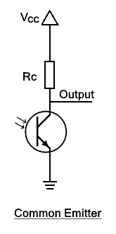
Common emitter: In this configuration, the collector is connected to the voltage source through a load resistor Rc and their output is taken from the collector as shown in the figure below. The output voltage moves from high to low state with the detection of light. It is a widely used configuration that acts as an amplifier.
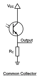
Common collector or emitter follower: in such configuration, the emitter is connected to the ground through load resistor RE and the output is taken from the emitter as shown in the figure below. The output voltage moves from low to high with the detection of light.
Types of Phototransistor
Phototransistors can be classified into bipolar junction transistor BJT and field effect transistor FET phototransistor.
BJT Phototransistor
BJT phototransistor is a more commonly used phototransistor. Therefore we have explained it above. It is available in both NPN and PNP designs. The light source controls the collector current. Its disadvantage is that it allows leakage current in dark conditions. However, it can conduct a large current because the current flow is due to both majority and minority charge carriers ( since the name bipolar). It cannot perform at high frequency but allow a large current with high gain.
FET Phototransistor
FET phototransistor is a field effect transistor having no junction and a channel that is sensitive to light. The channel can be either N-channel or P-channel. It has two terminals named source and drain. Construction-wise, drain and source are the same, they can be interchanged. The drain is positive with respect to the source. The incident light controls the drain current. It has a high switching speed allowing it for high-frequency applications. But it allows low current and low gain.
Related Posts:
- LED – Light Emitting Diode: Construction, Working, Types & Applications
- What is Photodiode? Types, Construction, Working & Applications
Parameters & Characteristics of Phototransistor
Since it has a similar design as BJT, it has similar characteristics.
- It has two terminals emitter and collector. The base terminal is physically not available since it is light-controlled.
- Some designs include a base terminal that should remain disconnected. Otherwise, it operates as normal BJT.
- The collector is maintained at a higher voltage than the emitter to make the B-C junction reverse and B-E junction forward bias.
- Under no light conditions, there is a flow leakage current called dark current. It depends on the temperature.
- Light striking the junction generates a base current that is proportional to the intensity of light. The base current is amplified into collector current with high gain.
- It has two operation modes active and switch mode. In active mode, it operates as an amplifier depending on light intensity. While in switch mode, it has “On” and “Off” states.
- The voltage across the collector-emitter junction can permanently damage it if it crosses breakdown voltage.
- Due to the large base and collector region, the B-C junction capacitance is large which affects its switching speed. Therefore they are not suitable for high-frequency applications above 250kHz.
Performance Parameters
There are certain parameters that define the performance of the phototransistor. These parameters must be kept in mind when choosing a phototransistor to provide cost-efficient performance.
Collector current Ic: it is the maximum allowed load current (collector current). Exceeding the load current amount this limit can permanently damage the phototransistor.
Base current: the base current indicates the current generated from the incident light. It depends on the area of the base region. However, increasing the area of the base region increases the capacitance the affects the switching speed.
Dark Current ID: it is the leakage current between collectorand emitter when there is no light. It is very small in milliamps. Ideally, it is meant to conduct no current. But due to temperature it never shut off completely. Dark current inversely affects the performance.
VCE breakdown voltage: it is the maximum voltage applied between the collector and emitter. If the applied voltage exceeds the breakdown voltage, the device is permanently damaged.
VEC breakdown voltage: it is the maximum allowed voltage applied between emitter and collector. It is relatively very lower than VCE breakdown voltage
Wavelength: Different photoconductive materials show different responses to a spectrum of wavelengths. They show high sensitivity and conversion efficiency at a narrow range of wavelengths. Therefore the wavelength of the incident light is very important to have higher energy conversion.
Linearity: Linearity means how linearly the output current varies with change in light intensity. Linear response is precise and error-free. Therefore it is necessary to know the linearity of the device.
Sensitivity: Sensitivity is the ratio of the change in output current to the change in intensity of incident light. To sense even small changes in light intensity, High sensitivity is required. It improves the performance of the device.
Response Time: the response time determines how quickly the output current updates with the change in incident light intensity. It is used to monitor sudden changes in intensity.
Rise and Fall Time: Rise time TR is the time it takes from 10% to 90% of its maximum value while fall time TF is the time it takes from 90% to 10%. Small rise and fall time determine quick response time.
Size and cost: The size and cost determines the economical value of the device. Low cost and compact size make it.
Design Parameters
Homojunction Structure: in such a structure, the whole device is made of a single material. such design is easy to fabricate and inexpensive. It allows a gain of 50 to several hundred. Usually, it is made of silicon.
Heterojunction Structure: it is made of different materials to provide high sensitivity and gain about 10,000. But they are quite complex to fabricate and costly.
Material: The martial determines the wavelength range of the phototransistor such as
- Silicon wavelength range is 190 – 1100nm
- Germanium wavelength range is 400 -1700nm
- Indium gallium arsenide wavelength range is 800 – 2600nm
- Lead sulfide wavelength range is 1000 – 3500 nm.
Collector Characteristics of Phototransistor
The following graph shows the relationship between the collector-to-emitter voltage VCE and the collector current IC at different levels of light intensity. The x-axis represents the voltage across collector and emitter while the Y-axis represents collector current IC.

Its characteristic curve resembles that of a BJT except the gain is controlled by the intensity of light. The collector current increases with light intensity. In no light conditions, there is a small leakage current or dark current.
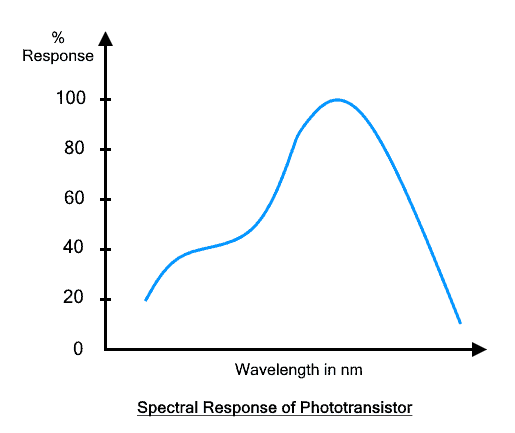
Spectral Response of Phototransistor
Phototransistors are made of photoconductive material that does not respond to all wavelengths but they show peak performance at a narrow range of wavelengths. The spectral response shows the relationship of wavelength with the percentage response of a phototransistor as shown below.
Photodarlington
Photodarlington is a modified phototransistor made from the combination of two phototransistors connected back to back to increase the gain ( sensitivity) of the device as shown in the figure. The configuration also increases the switching time. They are used for their high sensitivity.

Related Posts:
- What is Diode? Construction & Working of PN Junction Diode
- Types of Diodes and Their Applications – 24 Types of Diodes
Advantages & Disadvantages of Phototransistors
Advantages
Here are the advantages of phototransistor
- Phototransistor has higher sensitivity than a photodiode.
- It has a high current gain, especially the heterojunction design.
- It generates a large amount of current due to gain as compared to the photodiode.
- It has a fast response time and provides output instantaneously
- It is sensitive to different wavelengths including infrared IR, ultraviolet UV, and visible spectrum.
- It operates quietly as compared to an avalanche photodiode.
- It is highly reliable and stable.
- It has a small size, simple design, and is inexpensive.
- It is compact and can be fabricated several of them on sn IC.
- It can sense various light sources such as sunlight, flame, incandescent bulb, lasers, etc.
Disadvantages
Here are the disadvantages of phototransistor
- It has a low switching speed due to high junction capacitance (large base-collector area)
- It cannot handle high voltages like other optoelectronic devices such as thyristors and TRIAC.
- Voltage surges and spikes can damage it.
- It is not suitable for high-frequency applications like photodiode.
- It cannot detect low-intensity light.
- It is affected by electromagnetic energy.
Related Post: What is an Optocoupler or Opto-isolator – Working And Applications
Applications
A phototransistor is used for its high sensitivity and large current carrying capacity. Here are some applications of the phototransistor.
Light sensing: They are widely used to detect light and measure the intensity of light.
Automatic light control: it can automatically control the light in street or on the highway. it senses the sunrise and sunset and switches On or Off the connected lights on the circuit.
Object counter: it senses an object when it passes between it and a constant light source. It triggers the connected circuit when the object interrupts the incident light.
Opto-coupler: it electrically isolates two circuits and optically connects them using light pulses to protect low voltage circuits from high voltage circuits.
Punch card reader: it is widely used in punch card readers.
Shutter control: it controls the opening of the camera shutter based on the intensity of the light falling on its lens.
Alarms: it is used in burglar alarms by detecting the presence of a person passing through it. Fire alarm and smoke alarm also uses phototransistor.
Proximity sensor: it detects presence when something comes in its range such as in a smartphone that turns off the screen when it’s near your ear.
Infrared Sensing: sensing IR at night time allow it to use as a night vision device.
- Encoder
- Optical remote control
- Printer and photocopier etc.
Related Posts: