Half H-Bridge Inverter – Circuit, Operation, Waveforms & Uses
Waveforms and Operation of Half H-Bridge Inverter
What is Half H-Bridge Inverter?
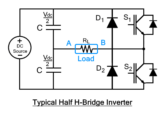
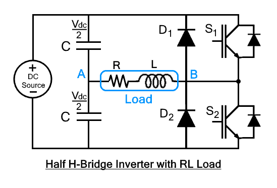
Half H-bridge is one of the inverter topologies which convert DC into AC. The typical Half-bridge circuit consists of two control switches, 3 wire DC supply, two feedback diodes, and two capacitors connecting the load with the source. Control switch can be any electronic switch i.e. MOSFET, BJT, IJBT, or thyristor, etc.
The circuit is designed in such a way that both switches must not turn-on at a single time & only one of the two switches will conduct. Each switch will operate for half period (T/2), providing half of the applied voltage the load (± Vdc/2). When both the switches are off, the reserved voltage across the load will be Vdc instead of Vdc/2. This is called a half-bridge inverter.
Some of the conventions in the given circuit are such that
- Current through S1 is i1, while the current flowing through S2 is i2.
- Output voltage and current are Vo and io
- T is the time period and switches are considered unidirectional.
Related Post: Types of Inverters and their Applications
Operation of Half H-Bridge Inverter with R Load
The operation of half-bridge with pure resistive load is the simplest. A purely resistive load does not have any storage component, so the circuit doesn’t need feedback diodes. The circuit with this load will be operated in just two modes.
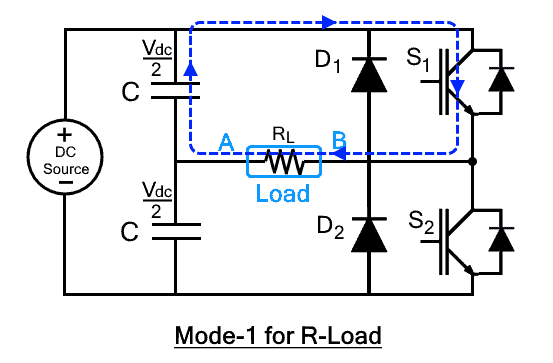
Mode 1: (0<t<T/2)
In this mode, S1 is turned-on from time interval t=0 to t=T/2 while S2 is turned off. As soon as S1 is turned on, the voltage across the load will appear. The output voltage across the load will be
Vo = Vdc/2
The current flowing through the switch S1 will be
Io = Vdc/2RL
Where RL is the load resistance. The current flow in clockwise direction as shown in the figure.
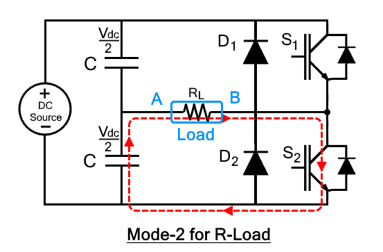
Mode 2: (T/2<t<T)
In this mode, switch S2 is turned-on from the time interval t=T/2 to t=T while S1 is switched off. Immediate switching of modes is avoided because it causes a short circuit. Due to this reason, S2 is turned-on with some delay after S1 is completely turned off. In this case, the output voltage will be negative as the current enters in the load from the opposite direction where output voltage will be
Vo = -Vdc/2
The current through S2 will be
Io = Vdc/2RL
The current flows in the reverse direction through the load as shown in the figure. Hence it shows that the half H-bridge has converted the applied DC into AC.
Waveform of Half H-Bridge with R Load
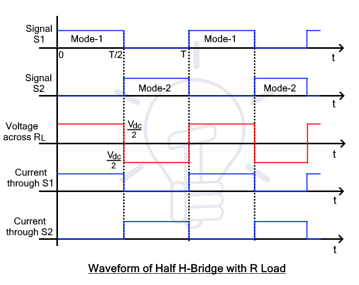
The first two waveforms show the pulses applied to the switches where each switch receives the pulse when the complementary switch is off. 3rd graph shows the voltage waveform across the load. This shows that the polarity of voltage changes w.r.t switching. The last two graphs show current through switches S1 & S2.
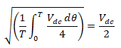
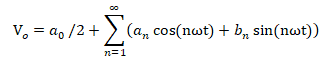
The root-mean-square (RMS) value of the output voltage can be calculated by
Fourier transform can be used to express the instantaneous voltage
As there is no DC offset so ao is zero and due to quarter-wave symmetry, all the components in are an zero. So, the contribution of bn will only remain & bn is given as

By putting the value of bn in Fourier series equation, we get

Vo = 0 for n=2,4,6,8…
ω is the angular frequency of the output voltage. The even harmonics of the output voltage are not present due to quarter-wave symmetry. Hence the result is
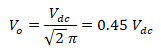
From here, the output voltage is approximately equal to half of the applied voltage.
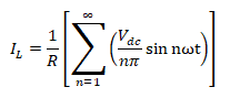
The current through the resistive load can be easily calculated out by just dividing the RMS voltage by its resistance.
Half H-Bridge Operation with L and R-L Load
The working operation of half-bridge for both L and R-L load is the same. As neither 100% pure inductive load nor pure resistive load exists in real life. A pure inductor has some value of ohmic resistance, so R-L load is more common in practice.
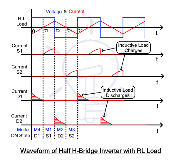
Here we will consider the working operation with RL load in a half H Bridge inverter. The working operation can be understood in 4 modes where 2 of the modes are used for controlling switches and 2 for the feeding back of the stored energy to the sources.
Terminal A and B are considered for sign convention across the load. Time interval when S1 triggered, A is more positive while B is more positive when S2 triggered. The shape of the current waveform and voltage waveform are both the same if the load is resistive. In case of RL load, both the current and voltage waveform will not rise at its peak points at the same time. The current will lag when the load is inductive dominant while voltage will lag in case of a capacitive dominant load.
The damping current will pass through feedback diodes when the polarity of both current and voltage is not the same. Diode D1 will conduct when the current is positive, and the voltage is negative. D2 will conduct when the voltage is positive while the current is negative.
The waveform is a bit different because the inductor resists the change of flow of current. For this reason, when switches are triggered to change the flow of current, the inductor will show resistance to the change. Hence the waveform differs.
These modes are discussed by considering that all switches are initially off and zero energy is stored in storage components.
- Related Post: Analysis of a Simple R-L Circuit with AC and DC Supply
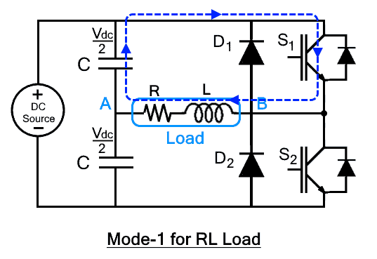
Mode 1 (0<t<t1)
In this mode, switch S1 will conduct from time interval t1 to t2. The current will start flowing from DC source to the load through s1 as soon as it is triggered. The current will enter through terminal B, showing that B is more positive w.r.t terminal A as shown in the figure. The source voltage will appear across the load which is Vdc/2 and current will gradually increase from zero to max. The inductor will store the energy as the polarity of both current and voltage is the same.
Mode 2 (t1<t<t2)
As switch S1 is closed, negative voltage (-Vdc/2) will appear across the load while the direction of flow of current will remain the same because the inductor will resist the change. In other words, the inductor will provide the stored energy, and D2 will provide the path for the current to flow form load to the source. The current through the load will gradually decrease till load current IL becomes zero. The reason is that the current flow due to stored energy in the inductor. As the inductor discharges, the current through the load becomes zero.
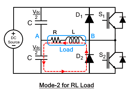
The main agent in this mode is feedback diode D2 which is also known as a freewheeling diode. It has two functions; one is to feedback the stored energy in the load into source while another is to reduce the di/dt spike generated by the inductive load. The freewheeling action of D2 can be more clearly visualized in the figure above.
Related Posts:
- 12V to 5V Converter Circuit – Boost and Buck Converters
- What is Boost Converter? Circuit Diagram and Working
- Buck Converter – Circuit, Design, Operation and Examples
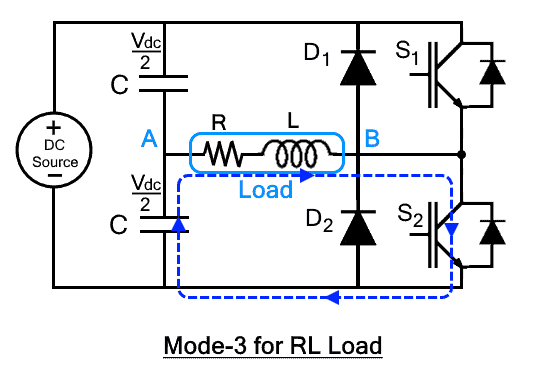
Mode 3 (t2<t<t3)
After completely discharging the inductor through the load, the current through load will become zero. At this movement, S2 is triggered. The current flow direction through the load will be reversed. After triggering S2, the current will start increasing and will achieve a negative peak. During this interval, both current and voltage are negative. So, the inductor will store the charge once again.
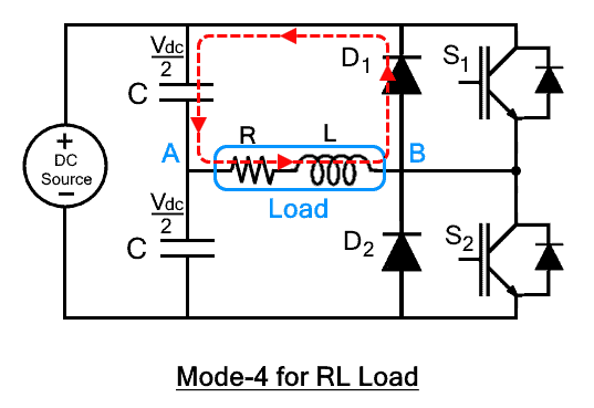
Mode 4 (t3<t<t4)
At time interval t3, the switch S2 is turned off. Positive voltage (Vdc/2) will appear across the load when S2 is turned off while the direction of the flow of current will remain the same. Diode D1 will provide the path and stored energy will feedback to the load. The current through load will gradually decrease until it becomes zero. The freewheeling action of D1 can be visualized from the following figure in this case.
Waveform of Half H-Bridge with L and R-L Load
As pure inductive load doesn’t exist, it must have some wire resistances and material resistance. Hence, more practical RL load is shown in the waveform rather than showing a theoretical.
The instantaneous load current IL for the pure inductive load can be calculated by dividing the output voltage with the impedance of the load (Z = R + jnωL)
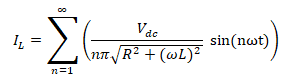
For RL (Inductive) load, the load current becomes
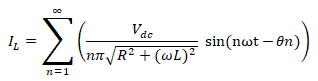
Where θn = tan-1 (nωL/R)
Related Posts:
Waveform Comparison of all Loads
The operation of half H-bridge inverter with an RLC load will remain the same as the operation of RL load with just a minute change. So, there is no need to explain the operation explicitly, but the difference can be seen from the figures of their waveform down below.
The operation and waveform depend on the value of inductance and capacitance in the RLC load. The operation of half H-bridge inverter with the RLC load is the same as the RL load.
As we know that in capacitor current leads & voltage lags & in inductor the voltage leads & current lags. So there are two cases in RLC load; inductive dominant RLC load & capacitive dominant RLC load. The former means the inductance is greater than the capacitance while the latter means capacitance is greater than inductor in the RLC load.
Therefore, If the inductance is dominant in an RLC load, the load current will lag behind the load voltage. And, if the capacitance is dominant in an RLC load, the load current will leads the load voltage. However, the phase shift will be negated to some extent by interference of capacitor (in inductive dominant load) & inductor (in capacitive dominant load)
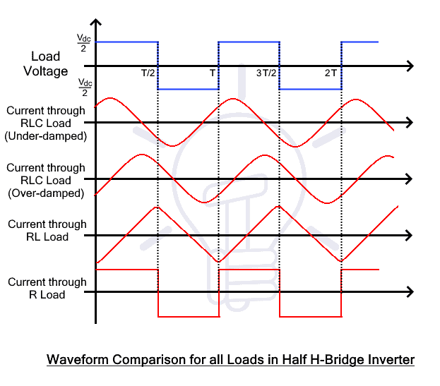
The operation and waveform vary for RLC load when the capacitor becomes dominant. In the capacitive dominant RLC load, the feedback diodes will conduct for different intervals of time due to the change in the current waveform.
Related Posts:
- Thyristor & Silicon Controlled Rectifier (SCR) – Thyristors Applications
- What is Rectifier? Types of Rectifiers and their Operation
- Difference between Inverter & UPS – Uninterruptible Power Supply
- Logic NOT Gate – Digital Inverter Logic Gate
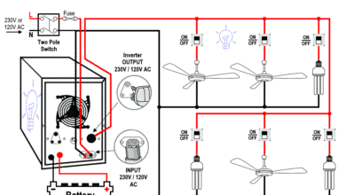
- Manual & Auto UPS / Inverter Wiring Diagram with Changeover Switch