Buck Converter – Circuit, Design, Operation and Examples
Buck Converter: Types, Circuit Design, Working, Modes of Operation, Examples, Losses & Applications
This article discusses Buck converter and all the important things about buck converter. All important points about buck converter i.e. operation, design, losses considerations and efficiency improvement of buck converter is discussed in this article. Let’s start from the very basics of buck converter to its designing.
Basics of DC-DC Converter
DC-DC converter is a converter which converts the DC voltage level of the input source into another DC voltage level. The DC-DC conversion can be done directly or can be done using alternative way. The alternative way is to invert DC input into AC and rectified back into DC after stepping up or stepping down the AC voltage using step-up or step-down transformer.
This way of transforming DC voltage level is way long and difficult. The short and direct method is to convert DC-DC directly using Boost converter or buck converter. The working of the boost converter is to boost the input voltage while buck converter is used for reducing the input voltage level.
There are two basic topologies in DC-DC converters that are isolated and non-isolated DC converters. The word isolated self-defines that input and output of the DC-DC converter is isolated by AC portion. Isolated DC-DC converters consist of three main parts that are inverter, transformer and rectifier.
The inverter for converting DC input voltage into AC, Transformer for stepping-up or stepping-down the AC voltage and finally the rectifier for converting back into required DC voltage. In contrast, the input and output of non-isolated DC converter are not isolated by AC part. In other words, a non-isolated DC converter converts DC input directly into DC output.
Examples of non-isolated DC-DC inverters are Buck, Boost, Buck-Boost, Cuk and SEPIC converter. In contrast, examples of isolated converters are Push-pull, Forward, Flyback, Half-Bridge and Full-Bridge converters.
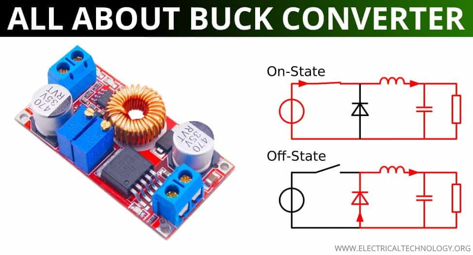
The main agent responsible for converting DC-DC conversion in non-isolated converter is a controlled switch. When the switch is ON; the input voltage appears across the load while the voltage appearing across the switch is zero. in contrast, when the switch is off, zero voltage appear across the load while all the input voltage appears across the switch.
The switch turns ON and turns off periodically which results in pulsating output. The output is then passed through filter which will extract the DC average value of the pulsating output. The DC average value is then controlled by the turn-on and turn-off time of the switch known as Duty cycle. Ideally the power loss is zero because the input power is equal to output power.
Ideally pure DC source is required for a DC-DC converter at input side i.e. DC current source and voltage source with no ripples and no AC components. The same requirement is also for the output of DC-DC converter. The output is required to be perfectly converted by converter with zero ripples and no AC components.
Practically the input of DC-DC converters has current ripples while their outputs have voltage ripples. Therefore, filters are required at both input and output ends. The filter at output is must for removing ripples and extracting average voltage.
Buck Converter
A buck converter steps down the applied DC input voltage level directly. By directly means that buck converter is non-isolated DC converter. Non-isolated converters are ideal for all board level circuits where local conversion is required. Fax machines, scanners, Cellphones, PDAs, computers, copiers are all examples of board level circuits where conversion may require at any level inside the circuit. Hence, a buck converter converts the DC level of input voltage into other required levels.
Buck converter is having a wide range of use in low voltage low power applications. Multiphase version of buck converters can provide high current with low voltage. Therefore, it can be used for low voltage high power applications. This article will discuss both low voltage low power converter and low voltage high power converter.
The efficiency of the converter can be improved using synchronous version and resonant derivatives. The other method of improving efficiency is to use Multiphase version of buck converters. The improvement of efficiency with multiphase inverter is discussed at the end of the article.
- Related Post: What is Boost Converter? Circuit Diagram and Working
Basic Topology of Buck Converter
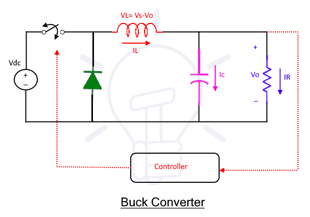
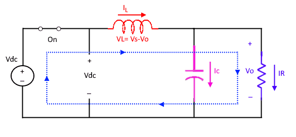
The basic buck converter consists of a controlled switch, a diode, capacitor and controlled driving circuitry. The switch controls the flow of input power into output by turning ON and OFF periodically. The time for which the switch is ON during the whole period is known as Duty cycle.
The value of duty cycle D ranges between 0 and 1. For D=0, zero voltage appear across load while for D=1, all the input voltage appears across the load. That’s why buck converter is operated for D greater than 0 and less than 1. The basic circuit diagram of buck converter can be seen below.
The average output voltage of Buck converter is controlled using two different ways i.e. PWM and PFM. In PWM (Pulse Width Modulation), the overall switch time T is kept constant while the turn ON time ton of the switch is varied. In contrast, the switching period time T is varied while the turn ON time ton of the switch is kept constant in PFM (Pulse Frequency Modulation).
Both PWM and PFM have some advantage and disadvantages. But PWM is preferred most of the time for operation of buck converter.
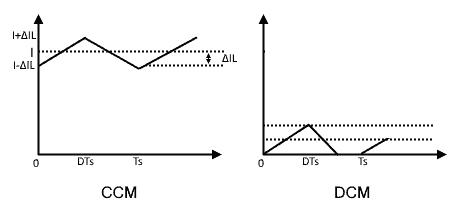
A buck converter operates in two types of conduction modes i.e. CCM and DCM. In CCM (Continuous Conduction Mode) the inductor current IL remains positive throughout the switching period. The inductor current IL never become zero through the switching period.
In contrast, the inductor current in DCM (Discontinues Conduction Mode) become zero for some time in switching period. Waveforms for both continuous and continuous conduction modes are shown in the figure below. All the discussion in this article is for CCM buck converter which is required for most of applications.
Modes of Operation in Buck Converter
As we have discussed in the previous topic that there are two modes of operation in buck converter i.e. CCM and DCM. In this topic it is discussed that how the converter operates in CCM and DCM modes.
The boundary condition between CCM and DCM is known as BCM, which will be discussed after. In addition, this topic discusses the properties of both CCM and DCM and how to change from one mode to other.
CCM (Continuous Conduction Mode)
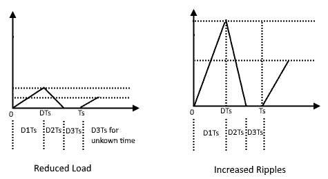
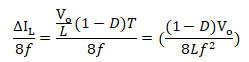
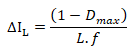
The converter is said to be operating continuous conduction mode if the load current never become zero during the complete cycle. If the buck is designed in CCM for higher load, then the converter may operate in DCM for lighter load. To understand its origin, let’s look at the inductor current ripples equation and load current. The inductor ripples ΔIL is
 The DC component is I=V/R
The minimum diode current is (I- ΔIL). It is to be notes that Load current I is depend on the load while ΔIL doesn’t depend on the load. We can see from inductor ripple equation that the value of inductor’s current ripples is inversely proportional to the inductance.
If the inductance value is reduced, then the ripple will increase. Further reducing the inductance value will increase the ripples such that ripples will become more than load current. At that time, the operation of converter will change from CCM to DCM because the load current will become zero for some instant.

Now, let’s check the case when inductor current is kept constant and Load Resistance is varied. Increasing the load resistance will reduce the load current. Let’s increase the load resistance till load current become equal to inductor ripples ΔIL.
The above graph will become as shown below. This is known as the boundary between CCM and DCM where further increasing the load will change the operation from CCM to DCM. The current become zero just for zero interval of time and then start increasing.
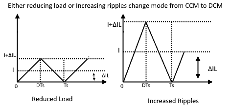
Further increasing the load resistance will reduce the load current further which will change the operation of buck converter from CCM to DCM. The operation mode immediately changes when load current reduces more than ripples. The condition for DCM is I < ∆IL. The following graph shows the DCM mode. The load current now prematurely drops to zero. By prematurely means that the current goes to zero before the switch is turned on.
Properties of CCM
Some of the properties of CCM are given as
- The converter that is stable in CCM mode will be stable in DCM mode too.
- The transmitting power in CCM is approximately proportional to the duty cycle D. whereas, the transmitting power in DCM is approximately proportional to the square of duty cycle D. From this statement we can see that DCM has advantage over CCM.
DCM Mode (Dis-continuous Conduction Mode)
More technically speaking, the DCM occurs due to switching ripples in inductor current. Or it occurs due to reversing the capacitor voltage polarity such that it violates the assumptions made for realizing the switch. In simple words, the inductor current ripples are more than the load current. So, during off time, the load current starts decreasing till it become zero.
Mostly in PWM buck converter it happens when both voltage and current of the circuit become zero for a short interval of time. During this interval, a new shape of the circuit forms which is normally not possible. This is known as DCM mode which is sometimes intentionally designed intentionally designed.
The overall DTs remain unchanged during DCM because the conduction of the signal is controlled by the control signal D. And this is independent of circuit operation however, DTs is divided into two new portions i.e. D2 and D3 as shown in the above figure. D2 and D3 are additional unknown parameters which make the calculation a little bit complex.
Properties of DCM
Some of the properties of the converter changes when converter starts operating in DCM. Some of those properties are given below
- Output impedance is increased
- Dynamics are changed after entering in DCM mode
- M becomes lo
 ad dependent
 - After removing the load, the control of output voltage may be lost
- On the switching node it may have huge ringing. As a result, it will have huge electric field interference for microseconds, or huge radiated EMI.
Related Posts:
- Analog to Digital Converter (ADC) – Block Diagram, Factors & Applications
- Digital to Analog Converter (DAC) – Types, Working & Applications
Working Operation of Buck Converter
The working operation of buck converter can be explained in two modes. The modes 1, when the switch is turned ON while the mode 2 when the switch is turned OFF. Both modes are explicitly discussed here.
Mode 1
By turning ON the switch, the diode will become reverse bias to the applied input. Therefore, all the input current will flow through inductor. Hence the DC input current Idc flowing in the circuit is equal to the inductor current.
IL= Idc
The inductor will charge during turn ON time. This current further divide into load current Io and capacitor current Ic.
IL= Ic + IR
The inductor voltage VLon during this period is the voltage difference between applied DC voltage Vdc and output voltage Vo.
VLon = Vdc-Vo
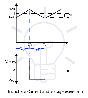
The average voltage across inductor VL is zero according to volt second balance. Recalling the duty cycle equation, the turn ON time ton is the product of duty cycle D and total time T.
ton= DT
the rippling current during turn-on mode can be find from inductor current voltage relationship
VL = Ldi/dt
di/dt = VL/L
By putting the value of VL we get
di/dt = (Vdc-Vo)/dt
ΔILon = Δton (Vdc-Vo)/L
By putting the value of Δton, the final form of the equation is as given
ΔILon = DT (Vdc-Vo)/L
The final result shows the current slop of inductor current during on time. The wave form shown given below shows the rippling current that first increase in ON time and then reduces with negative slop.
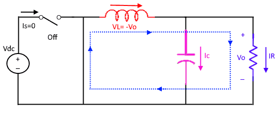
Mode 2
After turning OFF the switch, the mode 1 changes to mode 2. In this mode the polarity of inductor reverses and it start acting as a source. The current in this mode flows due to the stored energy in the inductor. The DC source is disconnected during this period. Therefore, the current flows in the circuit till the inductor discharges. The voltage appearing across the inductor is equal to the load voltage with negative polarity.
VLoff = -Vo
After turning OFF the switch, the polarity of inductor changes which make the diode forward bias. The anode voltage become more positive than cathode during this period and hence starts conducting.
The turn off time toff can be derived from turn on time ton in duty cycle.
toff = T – ton
toff = T – DT
The turn off time can be written in the final form as
toff = (1- D) T
The slop of inductor current can be found once again by voltage current equation of inductor.
VL = Ldi/dt = -Vo
di/dt = -Vo/L
ΔILoff = Δtoff (-Vo)/L
By putting the value of Δtoff, the final form of negative slop of the inductor current is as given
ΔILoff = T (1-D) (-Vo)/L
Minimum and Maximum Peak of Inductor Current
Minimum inductor current ILMIN and maximum inductor current IMAX are both most important terms in designing. Therefore, both minimum peak and maximum peak of the current need be found. Both ILMIN and IMAX can be found very easily according to previous discussion.
ILmin Calculation
ILmin= IL – |ΔIL|/2
By putting the values that we have been discussed in previous two modes of operation, the form of equation will become as given
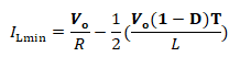
Further simplifying the above equation, the final form of the minimum inductor current can be achieved as given below.
![]()
ILmax Calculation
ILmax= IL + |ΔIL|/2
By putting the previously discussed values in the above equation, we will get
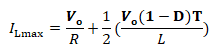
Further simplifying the above equation, we will get the final form as given below for maximum inductor current
Transfer Function of Buck Converter
The buck converter needs to be considered in steady state for finding transfer function. This consideration will make the calculations easy for finding transfer function. The average voltage across the inductor is zero in steady state according to volt second balance. Further, the inductor will act as a short circuit in steady state to a pure DC.
Mathematically
<VL> = VLonton + VLofftoff = 0
Where VLon is the voltage across inductor during turn ON time ton while VLoff is the voltage for turn OFF time. By putting the values of VLon, ton, VLoff, toff in above equation, the result will become
<VL> = (Vdc – Vo) DT + (– Vo) (1 – D) T = 0
Further simplifying will result
VdcD – VoD – Vo + VoD = 0
The final form of the transfer function is
Vo = DVdc
where the value of D ranges between 0 and 1. Therefore it shows that the average output voltage is always less than the applied input voltage.
Designing of Components and Ratings for Buck Converter
This section will discuss the designing of components used in buck converter with their ratings.
Inductor Designing for Buck Converter
This section will describe the important aspect of inductor required for buck converter. This includes two main ideas i.e. critical inductance and peak current rating of inductor.
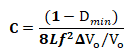
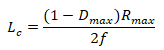
Critical Inductance
Critical inductance Lc is the minimum value of inductance at which inductor current reaches zero. Therefore, it is most important condition for operating buck converter in discontinues mode. In other words, the value of inductor is chosen below than critical inductance for operating buck converter in discontinuous mode.
The requirement is set by means of minimum percentage load. The other way is to set requirement by max ΔIL discussed previously. For operating buck converter in CCM mode, the inductor value is chosen more than critical inductance.
- L < Lc for operating buck converter in DCM
- L > 1.05Lc for operating buck converter in CCM
The critical inductance value can be easily found by using previously derived ILmin equation where setting ILmin =0 in the equation.
ILmin = 0 = IL-|ΔIL|/2
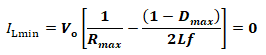
The value of critical inductance can be found directly by simplifying the equation. We get the following result after solving the above equation.
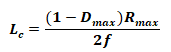 This is the most important equation for finding critical inductance which will decide the operation mode of buck converter. Where these quantities are selected as given
- Dmax is calculated input voltage for Lc.
- Rmax is calculated at minimum output current. Rmax = Vo/Iomin. Iomin is calculated and chosen such that to maintain CCM. It is chosen for 10% load with CCM. The value of Iomin may be specified by maximum ΔIL such that Iomin = ΔIL/2.
- f is the switching frequency which is normally chosen by the designer. The size of the critical inductance Lc is inversely proportional to switching frequency f. Therefore, choosing the high value of f will reduce the size of Lc which will reduce the size of buck converter.
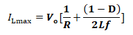
Peak Current Rating of Inductor
The peak current rating of inductor can be found using maximum value of the inductive current ILmax. The maximum inductor current occurs at maximum load. The peak current rating of inductor can be found using the equation of maximum inductor current as given as
ILmax= IL + |ΔIL|/2
The simplified form is given below which will define the rating the rating of inductor current.
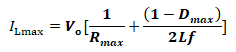
- Dmax is calculated from highest input voltage.
- The value of L must be chosen as discussed previously.
Switch Designing for Buck Converter
This section will discuss both current and voltage rating of a switch for buck converter.
Voltage Rating for Switch in Buck Converter
For ideal diode, the Vswitch-max is equal to Vdcmax while for non-ideal diode; Vswitch-max is equal to Vdcmax plus VF. the additional term VF is the maximum
- For ideal diode Vswitch-max = Vdcmax
- For non-ideal diode Vswitch-max = Vdcmax + VF
- Safety factor of 20% is used of at least 20%.
- The rating is Vdcmax for MOSFET
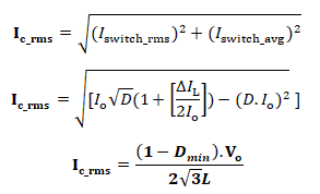
Current Rating for Switch in Buck Converter
The current rating for a switch is calculated based on average current. By drawing the switch current waveform, the average value of the current can be calculated. The average current for the switch is calculated here.
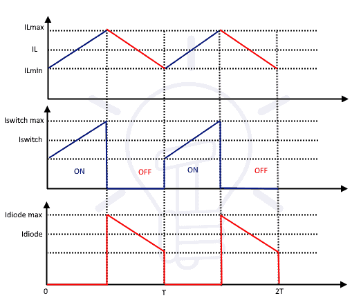
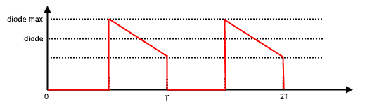
Overall inductor current is equal to switch current and diode current using KCL. During the turn ON time, the inductor current is equal to switch current while the inductor current is equal to diode current during turn OFF time. The waveform of switch current Iswitch, diode current Idiode and inductor current IL is shown below for turn ON and turn OFF time.
The average switch current <Iswitch> is
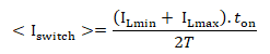
By putting the values in above equation, the result will become as given below.
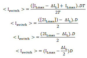
Further simplifying and putting the previously discussed value
<Iswitch> = <IL>.D
<Iswitch> = <Io>.D
The final form of the equation of current rating for the switch become
<Iswitch_max> = <Iomax>.D
Diode Design (Shotkey Diode) for Buck Converter
Shotkey diodes are preferred for the discharging of buck converters due to fast recovery action. These diodes are known as fast recovery diodes so preferable for high frequency operation i.e. buck converter. This section will discuss the current and voltage rating of shotkey diode for buck converter.
Voltage rating of diode for buck converter
VPRM or PIV (peak inverse voltage) is the maximum voltage across the diode. It is given in the data sheet of the component. For ideal switch, peak inverse voltage VPRM is equal to maximum input voltage VDCmax. For non-ideal case, VPRM is equal to VDCmax plus maximum forward voltage drop Vsw across the switch.
VPRM = VDCmax + Vsw
Where, the value of Vsw is calculated at maximum load current. For this calculation, it will allow the safety factor at least greater than 20%.
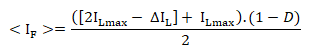
Current Rating of diode for Buck Converter
The same approach is adopted for calculating current rating for diode as it was adopted for the calculation of switch. The average forward diode current is calculated from the current waveform of the diode. As diode conduct during off time of the switch therefore, toff is considered in the calculation.
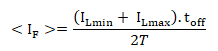
By putting values in the above equation, the result will become

Simplifying the above equation will result
By putting previously discussed values and simplifying, the result will become
<IF> = <IL> (1-D)
<IF> = <Io> (1-D)
This will lead to one of most important result that is given below
IFmax > I0max (1-Dmin)
The following wave form is the diode current wave form. It provides ease in finding average value.
Capacitor Designing for Buck Converter
This section will discuss the important parameter for a capacitor under which the capacitor can be operated in safe mode. Furthermore, the capacitor is designed such that the required functioned is performed.
Voltage Rating
The capacitor is designed and chosen such that the maximum capacitor voltage must withstand the maximum output voltage. Ideally the maximum capacitor voltage Vcmax is
As given as
Vcmax = Vo+ ∆Vo/2
Where, term ∆Vo shows the slope of output voltage.
The case is a bit different for particle capacitors. Practical capacitor disturbs the term ∆Vo/2 because practical capacitors have ESR (equivalent series resistance). The contribution shown by ESR for output voltage ripple is (ESR * ∆IL). This contribution made by ESR can be suppressed by using following methods.
- By Reducing ECR: reducing the ECR will reduce the voltage ripple disturbance. The ECR can be reduced by means of two methods. Either by connecting capacitors in parallel or by using capacitors that have low value of ECR.
- Reduce ∆IL: the value of can be reduced by increasing operational frequency or choosing bigger value of inductor L.
Minimum Capacitance According to Voltage
The designed capacitor will provide a path for AC ripples of inductor current while pure DC current will flow into the load. That is how the capacitor will act as a filter. The waveform of the capacitor current will look as shown below.

It can be seen form the below given waveform capacitor current w.r.t time that charge is the product of area of area and slop.
Q = area. Δ
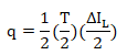
By putting the values and simplifying the result will become
As we know that q=CV. Therefore, C=q/v
By putting values in equation C=q/v

The final result for minimum capacitance will be as shown below
The value ΔVo is given in percent of peak to peak value of output voltage

RMS Current Rating and Minimum Capacitance According to Current
The capacitor is designed such that the maximum input voltage will be with stand by capacitor voltage. Ideally both are considered equal i.e. Vcmax = VDCmax while more realistically, capacitor has ESR (Equivalent Series Resistance). The ESR factor contributes to capacitor loss. The ESR factor can be reduced for better efficiency by two methods. Either by paralleling capacitors or by choosing capacitor with low ESR.
q = toff.D.Io
toff =(1-D) T
q = (1-D) T.D.Io
q = [(1-D).D.Io ]/ f
We know from the very basic equation that q = c.Δvdc
C = q/Δvdc
By putting the value of q in this equation, the result will be as given below
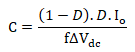
Io is considered as Iomax. Therefore, the above equation become
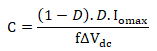
This is the required capacitance value while the RMS current rating equation can be found as
Summary Table
The following table shows all the important equations required for the designing of Buck converter.
| S.No | Parameters | Equation |
| 1 | Maximum switch current | <Iswitch_max>=<Iomax>.D |
| 2 | Maximum switch voltage | Vswitch-max = Vdcmax |
| 3 | Peak current rating of inductor |  |
| 4 | Critical Inductance | |
| 5 | Peak inverse voltage of diode | VPIV = VPRM = Vdcmax |
| 6 | Current rating of diode | IFmax > Iomax (1-Dmin) |
| 7 | Minimum capacitance | 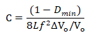 |
| 8 | RMS current rating of capacitor |  |
| 9 | Voltage rating of capacitor | Vcmax= Vo + ΔVo/2 |
Buck Converter Design for 12V to 2.5V, 1A
To design a buck converter that will convert 12-volt input DC to 2.5-volt output with 1A. For such conversion we have some known data and some parameters are required. Proper selection of components is must for successful conversion from 12v to 2.5 volt. This example will help to design buck converter for any conversion ratio.
Known Data for Designing Buck Converter
Applied DC input voltage Vdc = 12v
Required output voltage Vo = 2,5v
Iomax = 1A
Ioccm = 0.1A
%Vo = 1%
f = 50kHz
Solution for finding the Required Components
The duty cycle D can be found from the output input voltage ratio.
D=Vo/Vdc
D= 0.208
Inductor Value Finding
Critical inductance can be found from previously found equation
Lc=1.979 x10⁻⁴ H
The critical inductance can be chosen as
Lc=200 x10-6 H
The peak current rating can be found according to the equation

ILmax 1.099 A
The inductor rippling current ΔIL according to the equation is
ΔIL 0.198 A
Diode Values Finding
Vrrm =Vdc
Vrrm =12V
Forward diode current according to the given equation will be
IFmax = Iomax (1-Dmin)
IFmax = 0.792 A
MOSFET Values Selection
Maximum switch voltage according to the equation derived above
Vswitch-max = Vdcmax =12v
While maximum switch current
<Iswitch_max>=<Iomax>.D
<Iswitch_max>=0.208
Capacitor values selection
Minimum capacitance required for the converter according to the equation will be
![]()
C = 1.979 x 10⁻⁵ F
Near value for this required capacitance can be
C = 50 x 10-6
Voltage rating of capacitor
Vcmax= Vo+ ∆Vo/2
Vcmax = 2.513 V
![]()
- Related Post: 12V to 5V Converter Circuit – Boost and Buck Converters
Non-deal Buck Converter Loss Consideration
Losses for the buck converter must be considered when the efficiency estimation is required for it. Several major losses that are to be considered are given below and discussed briefly one by one.
- Static loss of MOSFET
- Switching loss of MOSFET
- MOSFET Gate Drive Losses
- Static loss of diode
- Switching loss of diode
- Inductor’s copper loss
- Capacitor’s ESR loss
Static loss of MOSFET
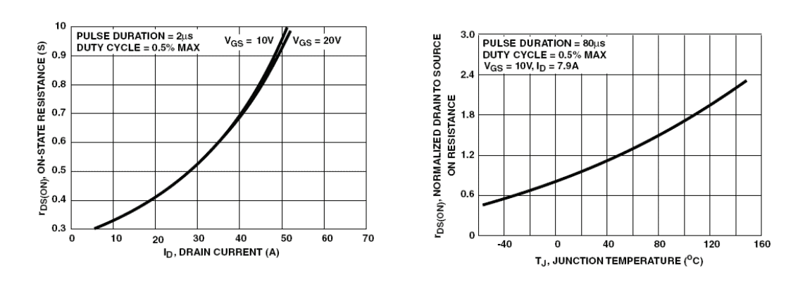
On Resistance of MOSFET RDSon directly impacts the static losses. This on resistance greatly contributes in over losses. The value of RDSon depends on two factors that are MOSFET’s junction temperature and applied voltage to the gate of MOSFET.
The two graphs given below show the exponential increase of on state resistance. The on-state resistance of MOSFETs increases with increase of Drain current due applied voltage to the gate. Pulse duration considered for this graph is 2µs, gate to source voltage VGS is considered 10V and duty cycle D is 0.5%.
The other graph shows the increase of on-state resistance with increase in temperature. Pulse duration considered for this graph is 80µs, gate to source voltage VGS is considered 10V and duty cycle D is 0.5%. Drain current in this case 7.9A.
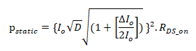
Static losses of MOSFET (P_static) for on-resistance RDS-on can be calculated by the given equation
Pstatic = (Iswitch_rms)2 . RDS_on
By recalling the value of Iswitch_rms and putting in the above equation, we will get the following result
Switching Loss of MOSFET
The switching losses of MOSFET depend on the overlapping pattern of voltage and current. As P=vi therefore, the power loss is directly proportional to their overlapping time. Switching losses are related with the transition time of the switch.
During the transition time, both current and voltage are non-zero. Therefore, the main switching losses are due to overlapping of current and voltage. This loss further increases with increase in frequency because losses occur both after turning ON and Turning OFF the MOSFET.
The given graph show that how losses occurs in transition states. The voltage across the switch approaches to zero with a specific slope while current across it increase. During this time losses occur. The same case is with turning OFF the switch.
During this time current approaches to zero with a specific slope while voltage drop across it increases. This is how transition losses occur during transition time.
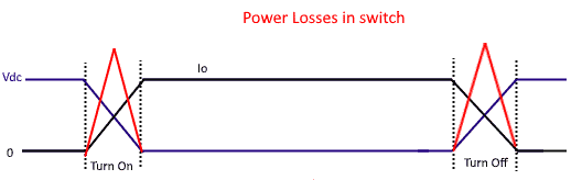
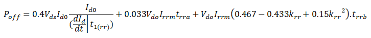
According to the above discussion the overall power losses Ploss is equal to the power losses during turn-on time and turn-off time.
Mathematically
Pstatic = Pturn-on + Pturn-off
We know that losses during turning-on time is
Pturn-on= ton.Io.Vdc/6T
While losses during turn-off time is
Pturn-off= toff.Io.Vdc/6T
By putting both these values in the above equation, we will get the following result

By taking common term, the final form for the overall switching losses will become
![]()
MOSFET Gate Drive Losses
These losses are considered due to the output capacitance Coss of the MOSFET. This capacitance is being charged when MOSFET is OFF which translate to the given loss
PCoss = ½ (CossVdc2f)
Whereas the gate drive losses come from two parameters i.e. the gate drive voltage Vgate and the total gate charge Qgate. By considering both, the mathematical form for gate drive losses is
Pgate = ½ (QgateVgate.f)
Static Loss of Diode
Losses that occur when diode is completely on or when diode is completely in off state. Static losses that occur when diode is in on state are known as forward static losses. In contrast, the losses occur in off state is known as reverse static losses.
Mathematically forward loss is the product of diode’s forward current (IF) and diode’s forward voltage (VF). For more precise value of the diode forward loss, the rms loss that occurs due to diode dynamic resistance, rd is added.
All these calculations were for forward losses. While losses for reverse state are
Preverse = VrIr (1-D)
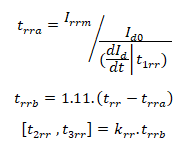
Switching Loss of Diode
This section will discuss the losses associated with diode connected in practical buck converter. The same is the case with diode as it is for switch discussed previously. This section will discuss losses associated in both turn-on time and turn-off time.
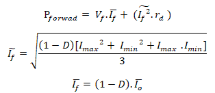
The losses associated in turn-on time are characterized by forward recovery time (tfr) and by low value of peak forward voltage (VFP). Both tfr and VFP can be find from data sheet where both tfr and VFP are plotted against dId(t)/dt. The factor (dId(t)/dt) is itself available for given set of conditions in the data sheet. By knowing above two value from the data sheet, the on-loss PON can be calculated from the given equation
PON = 0.4.(VFP-Vf ).tfr.If.f
The losses associated in turn-off time are associated with the time for which diode voltage and current overlaps. This overlap manly contributes in reverse recovery time.
This is really important equation for calculating turn-off losses in non-ideal case. Some of unknown values required for the above equation can be found from the following equations.
General Inductor’s Losses
There can be at most three inductors in buck converter that are storage inductor, coupled inductor and filter inductor. Therefore, the losses of all these inductors are considered in buck converter. In most of buck converters, the coupled inductor is not used but storage inductor and filter inductor are must. Therefore, losses of their two inductors are considered.
Some of the losses that occur in magnetic components are as given as
- Ohmic copper Loss: these losses are due to DC resistance and rms value of the current.
- Winding loss due to AC current: the AC current contribute in these losses by Skin effect, Proximity effect.
- Core Loss – Hysteresis & Eddy current loss: This occurs due to the AC flux in the core. Hysteresis losses are directly proportional to the frequency. The Eddy’s current losses are proportional to the square of the same frequency. The important equation used for calculating these losses is known as Steinmetz Equation (SE). This equation is given as
PV=K1.fa.ΔBβ
Above is the general form of Steinmetz equation whereas the modified form of this equation is as
PV=K1.faeq .ΔBβ
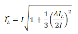
Inductor’s Copper Loss
There are two main type of losses associated with inductor i.e. inductor copper loss and inductor core losses. This section will discuss inductor copper loss while core losses are discussed separately.
Inductor copper loss, as its name suggests that these losses are associated with the winding of the inductor. As the winding is made of copper wire therefore, it is known as inductor copper losses. These losses are resistive in nature because the winding have some resistance. These losses are not significant that is why these are ignored for ideal buck converter while considered for more precise calculations.
Inductor copper losses occur due to the resistance of the winding. Therefore, inductor copper loss is the product of inductor DC resistance RL and inductor’s rms current I͠L.
PL = I͠L2.RL
rms current I͠L can be found according to the given equation below while RL is the inductor resistance.
Inductor’s Core Losses
Core losses of an indicator in buck converter are mainly affected by three factors i.e. flux swing B, switching frequency F and temperature. The general form of the formula for inductor core loss is given as
Core Loss = Core Loss/Unit Volume x Volume
Where the Core Loss/Unit Volume for the above equation can be calculated as
Core Loss/Unit = k1 x Bk2 x Fk3
k1, k2, and k3 are all constants that are normally provided by the core manufacturers. Values required for these constants need be as low as possible for low core losses. Some of well-known manufacturers and companies provide with very low values of these coefficients for better efficiency.
Capacitor’s ESR Loss
All real-world capacitors have (Equivalent Series Resistance) ESR. This resistance contributes to power loss in buck converter known as Capacitor ESR loss. the loss due to capacitor ESR can be found according to the following equation.
PESR = I͠c2.RESR
Where, this I͠c2 in the above equation is the capacitor rms current while ESR is the series resistance of the capacitor. The value of I͠c2can be found according to the previously discussed equations.
- Related Posts: Transformer Losses – Types of Energy Losses in a Transformer
Examples of Buck Design with Losses
A buck converter has already been designed in this article. But that example was for pure ideal buck converter which does not exist in practical life. This section will show how to use previously derived equations to compute the values of different components required for buck converter.
(Design of non-ideal Buck converter) Example 1
This example will show that how to design non-ideal buck converter for given parameters. We will design a non-ideal buck converter for the given parameters according to the previous discussion and derived equations.
Given parameters
Nominal output voltage of the system is
Vonom = 12V
Nominal input voltage of the system is
Vinnom = 24V
Maximum output power is
120W
Switching frequency is
Fs = 250 kHz
Maximum ripple percentage is
Vopp = 2%
Minimum percent CCM is
Iccm = 10%
Calculations for Designing
Nominal duty cycle for the non-ideal buck converter is
D = Vonom/Vinnom
D = 0.5
Inductor value selection: The critical inductance formula is a little bit different that is
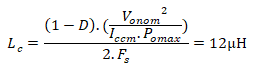
Conclusion: We have already discussed that the value of inductor must not be chosen less than Critical inductance. Therefore, the value of inductor can be any value greater than this critical value. Hence choosing Lo as
Lo = 200 µH
The DC resistance value of the inductor 200 µH can be measured though DMM. But we are assuming it to be 100mΩ.
RLo= 100mΩ
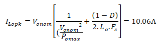
Calculating peak inductor current according to the above discussion is
Switch Selection:
The switch voltage is
Vswmax = Vinom = 24V
Switch current is as
Id = D.Pomax/Vonom
Id = 5A
Conclusion: According to above results we came to know that MOSFET IRF7471 40V 10A Rdson 13mO is the better solution.
Diode selection:
For proper diode selection, we need to know the values of two parameters i.e. diode Vrrm and diode forward current. We know that
Vrrm = Vinom
Vrrm = 24V
Diode Forward Current according to the given equation is as
IF = (1-D).Pomax/Vonom
IF = 5A
Conclusion: according to the above values, we came to know that Shotkey diode MBR3040 is the best solution. For further detail, see the data sheet of MBR3040.
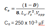
Choosing capacitor
For choosing the value of capacitor, we need to know the values of three parameters I.e. capacitor voltage rating, Capacitance Co and RMS current Rating.
We know that the value of capacitor voltage rating according to the formula is
Vcap = Vonom+Vopp.Vonom/2
Vcap = 12.12V
The capacitance Co is
RMS Current Rating can be found according to the given formula as
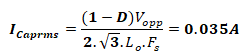
Conclusion: looking at the above results, we came to know that 25V 50uF capacitor is the best value of the capacitor to be chosen.
(Design of non-ideal Buck converter) Example 2
This example illustrates the design of buck converter which is maintained down to 10% of the 5A which is the full load current.
Given parameters
Output voltage of the system is
Vo = 12V
Input voltage of the system is
Vdc = 24V
Switching frequency is
Fs = 100 kHz
Output Vpp-ripple percentage is
ΔVo = 10. x10-3 V
Percent minload-CCM is
CCM = 10%
Full load current
Iomax = 10A
Time period Ts is the reciprocal of the switching frequency. Therefore, Ts = 1/100k
Calculations for Designing
Here we will calculate all the important parameters required for the designing of buck converter. First of all, it is required to find ideal on time and ideal off time.
The ideal on time of the switch is the ratio of output voltage and input voltage with the product of total periodic time.
ton = (Vo/VDC).Ts
ton = 2.5 x10⁻⁵ s
Minimum current required to maintain continuous conduction mode (CCM) is
Iomin = ccm.Iomax
Iomin = 1A
Inductor value selection:
We will find the value of critical inductance value which will decide the minimum value for which buck converter can be operated in CCM mode. The value must be chosen bigger than critical inductance value for operation in CCM mode. Let’s say 10% bigger value of critical inductance.
Lc = (VDC-Vo).ton/2.Iomin
Lc = 4.5×10⁻⁵ H
Conclusion: As we have discussed earlier that chosen inductor value must be greater than 10% of the critical inductance value. So, L=1.1Lc
L = 4.95 x10⁻⁵ H
The minimum output current value can be computed according to the chosen inductor value that is
Iomin = (VDC-Vo).ton/2L
Iomin = 0.909A
The next thing to be determined is ILmin and ILmax at minimum load. Initial guess for ILmin and ILmax were both 1A because we need ripples to be zero.
The given two equations in terms of ILmin and ILmax are
Iomin = (ILmax1+ILmin1)/2
(VDC-Vo).ton/L = ILmax1+ILmin1
Hence, by simplifying ILmin and ILmax at minimum load are
ILmin1 = 0A
ILmax1 = 1.818A
Hence the difference between both
ΔIL1 = ILmax – ILmin
Calculating output capacitor value
The approximate value of the ESR according to its equation is
ESR = ΔVo/ΔIL
ESR = 5.5×10⁻³ Ω
If we assume that Electrolytic capacitor is used, then
ESR*C = 65µs
Co = (65 x10-6/ESR) s
By putting their values, the equivalent result is
Co = 0.012F
Conclusion: The nearest standard value of the capacitor to the calculated one is 15×10-3. Therefore, choosing output capacitor Co=15 x10-3
Total ripples calculation
For calculating total ripples, we need to find ripples due to two factors i.e. Ripples due to capacitor charge discharge and Ripples due to Capacitor’s ESR. These calculations are performed individually, and their addition gives total ripples. For calculating all these values, we need to recalculate the value of ESR for chosen capacitor.
ESR = (65 x10-6)/Co s
By putting values and simplifying, we get the result
ESR = 4.333×10⁻³
The value of ripples due to capacitor charge and discharge is
ΔVc = ( ΔIL.Ts)/8Co
The result of above equation, by putting values in it is
ΔVc = 1.515×10⁻³
The value of ripples due capacitor’s ESR is
ΔVESR = ΔIL.ESR
ΔVESR = 7.879 x10⁻⁴ V
Value of Total ripples is the sum of ripples due capacitor charge and Discharge and ripples due to Capacitors ESR.
ΔVtot = ΔVc+ ΔVESR
Efficiency improvement
The efficiency can be improved by choosing the correct value of components used in buck converter. The efficiency can be improved further by applying the discussed strategies to the following components.
By Capacitor
As it is discussed previously in this article that equivalent series resistance (ESR) of the capacitor directly contributes in power losses. Therefore, the losses can be reduced by reducing ESR. In other words, reducing ESR will reduce power losses which will increase efficiency.
Another way of reducing power losses and increasing efficiency is to use paralleling capacitors method. Using this method, over all capacitance will be increased while it will reduce ESR. Reducing ESR is the alternate way of saying that efficiency is increased.
Lower Inductor Current Ripple
The efficiency can be increased by reducing rms losses occurs both in inductor and output capacitor. These are magnificent losses and must be reduced for better efficiency. There are a lot of strategies for reducing inductor current ripples.
The more common solution to reject ripples is to use reservoir capacitor. This solution is for rejecting ripples from going to the output but the losses due to ripples still occurs.
The more practical solution is to increase switching frequency or to increase inductance. This will reduce inductor ripple, but it will increase losses due to frequency. The reason is that frequency is also directly proportional to losses. There is always tradeoff between both.
Now, if inductor value is increased instead of increasing frequency then the DC resistance of the wire increases. As the resistance value is directly proportional to the length of the wire of the winding. Therefore, choosing big value of inductor will increase the losses due to DCR.
Lower Gate Drive Voltage
By reducing the gate drive voltage, the power losses that take place there can be reduced. In other words, the efficiency of the system can be increased.
Use of Synchronous MOSFET
Using synchronous MOSFET instead of diode can improve efficiency. This improves the efficiency much better for low voltage and high current. This synchronous Rectification is done by replacing freewheeling Schotkey diodes with MOSFETs.
This procedure is especially beneficial for high current and low duty cycle applications. The problem still didn’t overcome, even by replacing Schotkey diode with MOSFET. The final problem can be solved by replacing the body diode with Schotkey diode. The reason is because body diode is slow due to its dead time.
In short, the whole concept is to replace freewheeling shotkey diodes with MOSFET and then Schottkey diode is connected across the MOSFET. The combination of both MOSFET and Schottkey is FETKEY for example IRF7326D2.
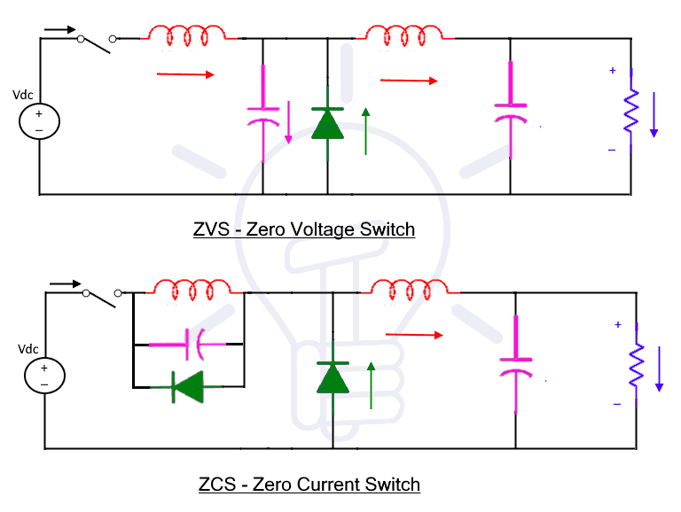
Soft switching
Soft switching prevents hard switching which means that it prevents the overlapping of current and voltage of the switch during turn-off and turn-on transition. This will significantly improve the converter efficiency because we have already discussed the relation of switching frequency and losses.
Resonant circuit is used to change shape of the signal. Using this circuit, current or voltage waveform goes to zero at the time when switch is initiated. This will reduce the switching losses almost near to zero.
There are a lot of Quasi-resonant buck topologies available such as Zero Current switching and zero voltage resonant buck converters. Zero Current switches operated with a constant on time control while with constant off time control the zero-voltage switch can be operated. Both ZCS and ZVS techniques are conventionally employed soft-switching methods.
These converters have the ability to shrink the power losses due to switch to zero by shrinking voltage or current to zero during transition time. Reducing the power losses will increase efficiency as efficiency and losses are inversely proportional to each other.
The circuits for both ZVS and ZCS are given below.
PWM Controller
Current mode controller is preferred because it has so many advantages. Some of the advantages are discussed here.
- Line Rejection
- A lot of input noise can be attenuated by the close current loop
- The ripples attenuation is usually adequate even with moderate gain in the voltage feedback loop with current mode control.
- Far more gain is required for Voltage mode control in the main loop to achieve the equivalent performance as it is achieved in current mode
- CCM and DCM operation
- To design a compensator with voltage mode that can perform well on both CCM and DCM is impossible.
- With current mode, there is no problem in the crossing the boundary between two operation modes i.e. CCM and DCM.
- It has a major advantage due to optimal response in both modes. It allows to operate the power stage much more efficiently.
- Easy compensation
- With voltage mode, since the filter resonant frequency requires a type 3 compensator for stabilizing the system. Therefore, the phase drops very sharply.
- Current mode resembles a single mode system, since we have noticed that the current loop controls the inductor.
- Using this the converter can be controlled very easily because it improves the phase margin to high extent.
- Looking at above points, type 2 compensator is adequate. Using this the designing process can be greatly simplified.
- Cross over must be more than the resonant frequency for voltage resonant frequency.
Lay Out Consideration
The following needs to be considered while lay out.
- Keep Trace inductance low
- to keep the trace inductance as low as possible. It is preferred to reduce the trace inductance by reducing length not by increasing length for the critical path. The critical path is the path of switch and diode.
- Noise spikes may appear to the controller chip, and in output and input.
- A current probe will introduce additional inductance. Therefore, avoid using it for diode and switch.
- Provision of input decoupling
- Provision of very good input decoupling because capacitor of input is in critical path. These capacitors are also known as bypass capacitors because they bypass the source when needed.
- In this case small ceramic capacitors are used. One from switch to the ground and another from the supply end to the ground. These capacitors are used beside the usual bulk capacitor.
- Provision of decoupling with ceramic capacitors
- Using a small ceramic capacitor provide good decoupling between ground pins and output.
- Use shielded inductor
- It is better to use shielded inductor and to keep its position away from the feedback trace and from the controller.
- Dedicating one layer for ground in multilayers
- It is better to dedicate one layer for the ground in multilayer boards.
- Keep short trace for feedback
- For minimizing the noise, the feedback trace must be kept as short as possible.
- Place the feedback trace away from the noise sources, as far as possible.
Multiphase Buck Converter
This technique overcame the deficiency of single-phase traditional buck converter. Since the traditional single-phase buck converter has single switch, diode and inductor. therefore, these components have current limitations and cannot be operated beyond those limits.
For higher power applications, the system needed to be operated for high current, but all these components have limitations. The best possible solution is to use multiple single traditional buck converters. This technique is known as Multiphase buck converter and can be used for low voltage high current applications.
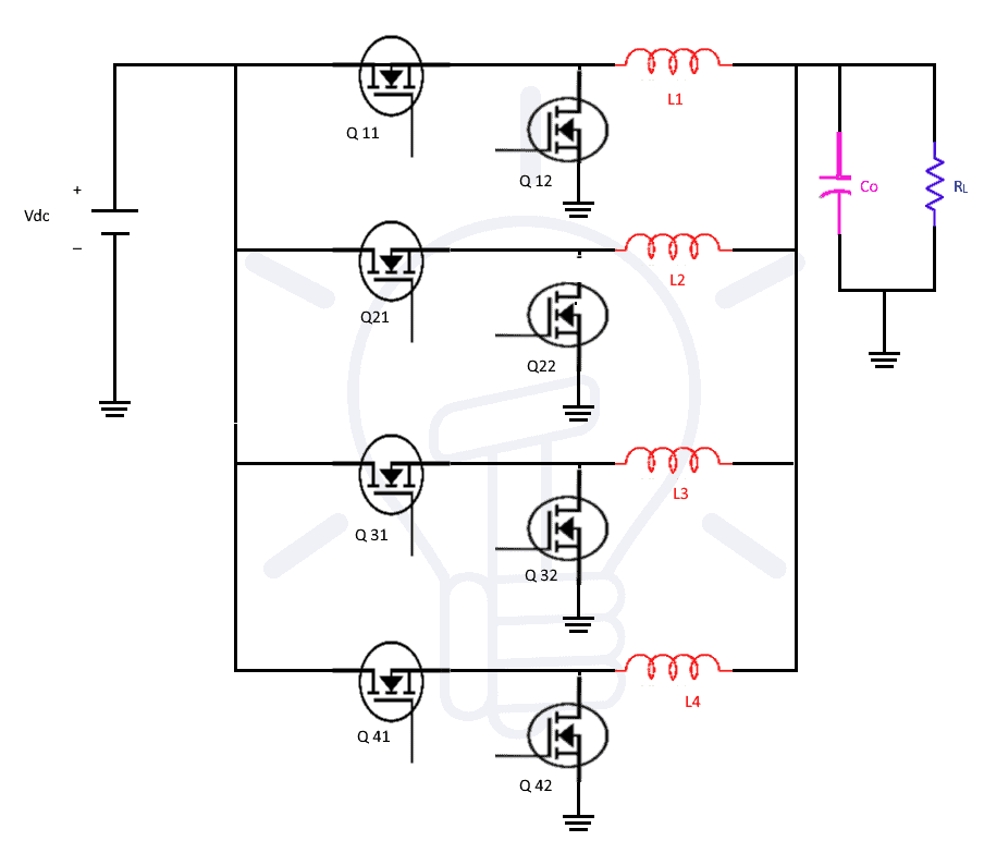
Above is the circuit diagram of Multiphase buck converter. It can be seen from the diagram that it is a simply the connection of buck converters in parallel. All their inputs are common to each other as their outputs and then connected to filter. The filter will filter most of ripples and will pass the DC power to the load.
This technique can be of the great use in the future since the next generation processors and ASICs require higher currents, low voltage and faster dynamic response.
It needs to be operated with great efficiency and power management solutions. In short, this technique will have a higher demand due to the meet the demand of increasing power density due to higher operating frequency and higher efficiencies. This technology is emerging to compete against coming power requirements.
Lower power level with high density applications can be managed with 2 phase solutions while high power levels may require up to 4 phase solutions or even more than that. The reason is again the limitations of components and other limitations of buck converter. So, for high density applications, higher phase solutions are required.
Related Posts:
- Difference between Inverter & UPS ( Uninterruptible Power Supply)
- Difference Between Online UPS and Offline UPS & Which One is Better?
Advantages of Multiphase
Even though there are a lot more advantages of multiphase technique but there are few them mentioned and discussed in this article. Some of the advantages are given as
- Better Efficiency
The best power efficiency can be achieved by the conversion in a single stage rather than converting in double stages.
For example: 24V need to be converted in 1.2V using a two-phase forward converter at 100W. The current will split equally in two phases in two phase conversion. Therefore, the losses will be reduced by 50% since we know that losses in switch is ×R. Secondly, lower peak current will reduce the turn on and turn off losses. As a result, the overall efficiency will be increased.
- Input/output ripples reduction
The switching frequency is increased by Multiphase PWM controllers. The switching frequency is directly proportional to the number of phases. The resulting frequency of Multiphase is equivalent to the PWM clock frequencies of individuals inverters time the number of phases.
For higher operating frequency the size of inductor can be reduced, and small input output capacitor is required. This is one of the main advantages of multiphase because a single buck converter is restricted to some limited frequency.
The frequency of individual buck converter cannot be increased more than rating frequency due to it its components frequency. But, in multiphase technique the number of phases can be increased as much as required. Hence, the operating frequency can be increased to desired level. The increasing frequency will reduce the size of inductor and capacitor size. In other words, reduced size will reduce the price and size.
- Better thermal management
AS discussed in the previous topic that frequency is inversely proportional to the size of inductor. Now, the small inductor will improve the dynamic response. In other words, the small impedance due to small inductor will allow changing the current fast.
- Ease of manufacturability
Automated assembly and small form factor are required for next generation designs. Next generations designs denied the use of bulky inductors, transformer and capacitors and hand soldering.
Related Posts:


Eectrical & Electronics engineering advance technology news required for education purpose.