Full Bridge Inverter – Circuit, Operation, Waveforms & Uses
Construction and Working of Single Phase Full Bridge Inverter (R-L-C Load)
What is a Full Bridge Inverter ?
Full bridge inverter is a topology of H-bridge inverter used for converting DC power into AC power. The components required for conversion are two times more than that used in single phase Half bridge inverters. The circuit of a full bridge inverter consists of 4 diodes and 4 controlled switches as shown below.
These diodes are known as freewheeling diodes or feedback diodes because these diodes feedback the stored energy in the load back into the DC source. The feedback action happens only when load is other than pure resistive load. The controlled switches for Full-bridge inverters can be BJT, IJBT, MOSFET or thyristors. Controlled switches considered in this article are thyristors.

The general concept of a full bridge inverter is to alternate the polarity of voltage across the load by operating two switches at a time. Positive input voltage will appear across the load by the operation of T1 and T2 for a half time period. The polarity of voltage across load will be changed for the other half period by operating T3 and T4.

This article is about the working operation and waveform of a single-phase full bridge inverter for R load, RL load and RLC load. The comparison of all loads is given at the end of this article.
Operation of Full Bridge with R Load
The working operation of Full bridge for pure resistive load is simplest as compared to all loads. As there is not any storage component in the load so, only control switches operate while feedback diodes do not operate through the operation of the inverter. Only two modes are enough for understanding the working operation of a full bridge inverter for R load.
Mode 1
Consider all the switches are initially off. By triggering T1 and T2, the input DC voltage (+Vdc) will appear across the load. The current flow in clockwise direction from source to the series connected load. The output current across the load will be
Io=Vdc/RL
Where RL is the load resistance, While the output voltage across the load will be
Vo= Vdc
Mode 2
Thyristors T3 and T4 are triggered immediately after completely commutating T1 and T2. The polarity of voltage immediately reverses after switching complementary switches T1 and T2 with T3 and T4. The DC input voltage across the load appear with the negative voltage which
Vo= -Vdc
While the output appearing current is
Io = – Vdc/RL
The current in anti-lock wise direction flows from source to load through T3 and T4 as shown in the figure.
- Related Post: Types of Inverters and their Applications
Waveform of Full Bridge with R Load
The current flowing through load and voltage appearing across the load are both in square wave form as shown in the third wave of the figure. The switching pattern is shown in the first two waves. Third wave shows the voltage across the load while the last two waves show the current flowing through the switches.
 The root-mean-square (RMS) value of the output voltage has been calculated from the equation as given
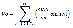
Fourier transform is used for expressing instantaneous voltage
As all the even harmonics are absent because the waveform of the output voltage is half-wave symmetric. So, the above equation just shows the odd harmonics. All the even harmonics are absent including average voltage across the load.
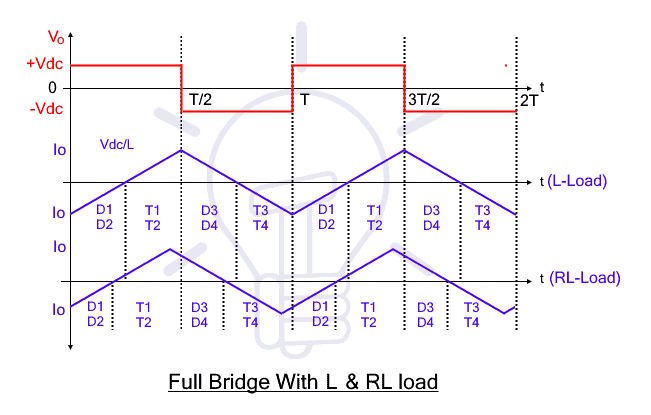
Full Bridge Operation with L and RL Load
The working operation of Full bridge for both L load and RL load is exactly the same with a slight shift of phase angle. Secondly, a pure inductive load does not exist as the resistance of the winding is included. Therefore, the operation of RL load is explained in this article.
The working operation for both L and RL can be interpreted in 4 modes. The 2 extra modes show the freewheeling action. The polarity of voltage across the load does not change immediately. The polarity remains the same due to the free-wheeling action.
The feedback diodes will conduct the damping current to the source from load when the polarity of voltage and current is not the same. Diode D1 and D2 will conduct when voltage is positive and current is negative. The damping current will continue to flow till the negative current through the load gradually reduces and finally approaches to zero. Then after, thyristor T1 and T2 are triggered so the polarity of current and voltage become positive and feedback diodes stop conducting. The other two diodes, D3 and D4 immediately start conducting as soon as T1 and T2 and commute.
These modes of operations are discussed by taking two assumptions.
- All the switches are initially closed.
- There is initially zero energy stored in the load.
Related Posts:
- Boost Converter? Circuit Diagram and Working
- Buck Converter – Circuit, Design, Operation and Examples
Mode 1 (t1<t<t2)
In this mode thyristor T1 and T2 will conduct from time interval t1 to t2. Thyristors T1 and T2 will conduct current from source to load as soon as these thyristors are triggered. After triggering the Whole input voltage will appear across the load with positive polarity while current will gradually increase till it achieves maximum peak. The current does not rise to the peak immediately as it rises in pure resistive load because the inductor resists the change.
The inductor will store energy in this mode. The reason behind it is that the polarity of voltage and current is the same.
Mode 2 (t2<t<t3)
In this mode, feedback diodes D3 and D4 will conduct the stored energy in the load back to the source. The feedback diodes will immediately start conduction by commutating thyristors T1 and T2. These diodes also reduce the di/dt spike.
Negative voltage will appear across the load as soon as previously triggered thyristors are commutated. The polarity of current remains the same, but it gradually decreases till the current flowing through load becomes zero. As the current flows due to the stored energy therefore, the current stops flowing when stored energy approaches to zero.
Mode 3 (t3<t<t4)
Thyristors T3 and T4 are triggered immediately after the complete discharge of inductive load. By triggering T3 and T4, the current starts to flow in the opposite. The current gradually increases till it achieves the negative peak.
During this interval, both current and voltage are negative. Therefore, inductive load charge once again.
Mode 4 (t0<t<t1)
The feedback diodes D1 and D2 will conduct in this mode. These diodes will start conducting immediately after commutating the previously triggered T3 and T4. The voltage polarity.
Related Posts:
- Difference between Inverter & UPS ( Uninterruptible Power Supply)
- Difference Between Online UPS and Offline UPS & Which One is Better?
Waveform of Full Bridge with L and RL Load
The voltage waveform in both L and RL load is square wave while the current wave in both loads are triangular.
Full Bridge with RLC load
In this topic, the response of RLC (Resistive, Inductive and Capacitive) load is discussed. The RLC load shows two types of responses. The response may be overdamped, or it may be underdamped. Both these responses are briefly discussed here.
RLC Overdamped Response
In this case, the inductive impedance is dominant with respect to capacitive impedance. Therefore, its response is more like RL load response with a slight voltage shift in the current voltage waveform. The voltage leads while current lags in RLC load with overdamped response. There is no need to explain it again as the working operation is more like RL load. The working operations are exactly the same as the RL load that Thyristors will conduct when current and voltage have the same polarities while diodes will conduct when current and voltage have opposite polarities.
The conduction time of diodes and switches are different. As, thyristors will conduct for T/3 period which is more than the conduction time of thyristors for RL load. more time with respect to RL load. diodes will conduct for T/6 period which is less than the conduction of RL load The output waveform of the current will be nearly sinusoidal wave with the use of a filter.
Mode 1 (T1 and T2 Conduct)
Feedback diodes are conducted initially. After triggering thyristors T1 and T2, the polarity of current reverses and load starts charging itself from source. During this mode, the current gradually increases in a positive direction till it achieves maximum peak. After achieving the maximum peak, the load current gradually decreases till the anode current becomes zero. The zero-anode current naturally commutates the thyristors T1 and T2. These thyristors conduct for T/3 of total time.
Mode 2 (D3 and D4 Conduct)
The mode changes from mode 1 to mode 2 after T1 and T2 are commutated. In this mode feedback diodes D3 and D4 start conducting. These feedback diodes keep conducting till thyristor T3 and T4 are triggered. The feedback diodes will conduct to the T/6 of the full time.
Mode 3 (T3 and T4 Conduct)
The direction of the flow of current through the load changes after triggering thyristor T3 and T4. In this mode, both the current and voltages are negative. Therefore, the load is charged throughout this period.
Mode 4 (D1 and D2 Conduct)
The feedback diodes D1 and D2 start conducting after commutating Thyristors T3 and T4. These feedback diodes will conduct if the load is fully discharged in the source.

RLC Underdamped Response
The RLC shows the underdamped response when the capacitor is dominant with respect to inductive impedance. Therefore, its working operation is a bit different and it needs to be discussed separately.
As the capacitive impedance is dominant in the load. Therefore, the load current leads while the load voltage lags. The working operations is briefly discussed in 4 modes;
Mode 1 (D1 and D2 Conduct)
Initially thyristors T1 and T2 are in conducting mode. After the current through thyristors approaches zero, the current direction through the load is changed and feedback diodes D1 and D2 start conducting. The time duration of mode1 is considered from the time when feedback diodes start conducting till these feedback diodes stop conducting. The conduction time is comparatively smaller as compared to RL load which T/6 of the total time.
Mode 2 (T3 and T4 Conduct)
After triggering thyristors T3 and T4 the voltage polarity reverses. The current direction is already in reverse direction. As both current and voltage are in reverse direction. Therefore, the RLC loads charge through-out this mode. The load charges for T/3 time where T is the time period.
Negative voltage i.e. -Vdc appears across the load while current gradually increases till it reaches the maximum negative peak. After touching the maximum negative peak, the load current gradually decreases till it becomes zero.
Mode 3 (D3 and D4 Conduct)
The feedback diodes D3 and D4 immediately start conduction after thyristors are being commutated due to zero anode current. In this mode the feedback diodes D3 and D4 start feeding the source from the stored energy in the load.
The polarity of load current has been changed already after switching from mode 3 to mode 4 while the polarity of voltage remains negative.
Mode 4
Thyristors T1 and T2 are triggered when anode current reaches sufficient current level. The polarity of load voltages changes i.e., input voltage appears with positive polarity. The load will charge once again due to the same polarity of current and voltage.

Waveform Comparison for all Loads

- Related Post: Logic NOT Gate – Digital Inverter Logic Gate
Parameters Comparison of Full Bridge of all Loads
| Parameters | Pure Resistive Load | Pure Inductive Load | RL Load | RLC Load |
| Output voltage Vo | Square wave | Square wave | Square wave | Square wave |
| Output current Io | Square wave | Triangular wave | Exponential wave | Sinusoidal wave |
| Conduction time of each switch | 180o or T/2 of full period | 90o or T/4 of full period | 120o or T/3 of full period | 120o or T/3 of full period |
| Conduction time of each diode | 180o or T/2 of full period | 90o or T/4 of full period | 60o or T/6 of full period | 60o or T/6 of full period |
The output current and voltage wave of RLC load differs with respect to the damping ratio. For ζ>1 full bridge inverter for RLC load shows overdamped response, while for ζ<1 the inverter shows underdamped response. The response is overdamped for XL>XC while for XL<XC shows underdamped response.
| Parameters | XL>XC (Overdamped Response) | XL<XC (Underdamped Response) |
| ζ |  |
|
| R |  |
 |
| ωn |  |
|
Related Posts:
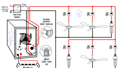
- How to Connect Automatic UPS / Inverter to the Home Supply System?
- Manual & Auto UPS / Inverter Wiring Diagram with Changeover Switch
- How to Wire Solar Panel to 120-230V AC Load and Inverter?
- Types of AC Drives & VFD
- Types of DC Drives
- What is Rectifier? Types of Rectifiers and their Operation
- 12V to 5V Converter Circuit – Boost and Buck Converters