Difference Between NPN and PNP Transistor
What is the Main Differences between NPN & PNP Transistor?
Transistors are the most abundantly used component in electronic devices. Transistors are mainly divided into two subtypes i.e. Bipolar Junction Transistor (BJT) and Field Effect Transistor (FET). BJTs can be further divided into two types based on their construction known as NPN and PNP transistors.

Before going into the differences between NPN & PNP, we are going to explain the basics of the transistor.
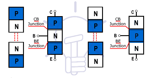 A BJT Transistor is formed by the combination of alternating layers of P and N-Type semiconductor material. There are two possible combinations. It is if either N-Type material is sandwiched between two P-type materials to form a PNP transistor or if P-Type material is sandwiched between two N-Type materials to form NPN Transistor
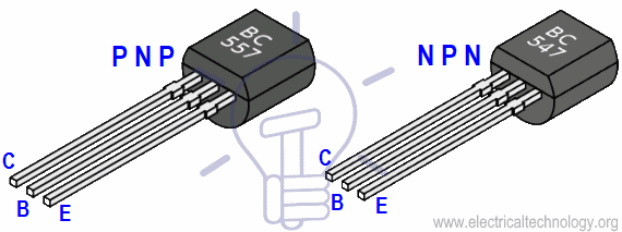
Here are the Pinouts of BC-547 NPN and BC-557 PNP Transistor respectively.
Related Posts:
- PNP Transistor? Construction, Working & Applications
- NPN Transistor? Construction, Working & Applications
NPN Transistor
An NPN Transistor is formed by the combination of two N-Type materials and one P-Type material. where the P-Type material is sandwiched between these two N-Type. The central P-region is the thinnest layer of all which is also known as the Base. One of the N-regions which is the thickest layer of all but is lightly doped is called collector while the other N-region is the comparatively thinner but heavily doped as compared to the collector is called emitter.
 The three terminals Collector, Base and Emitter each rise from N, P and N-Type material respectively. The Collector and emitter has electron as majority charge carriers while the Base has holes has majority charge carriers. On the contrary, the collector and emitter has holes as minority charge carrier while the base has electrons as minority charge carriers.
The base is a thin P-Type layer having the majority of holes. Applying a positive voltage with respect to the emitter will push electrons in the base (p-region). As it is thin and lightly doped, the electrons combine with holes resulting in penetration in the depletion region that causes the electrons to flow from the collector terminal to the emitter terminal.
Therefore, in the NPN transistor, applying a positive pulse at the base causes a current which is in the direction from the collector to the emitter. While the current is directly proportional to the base current.
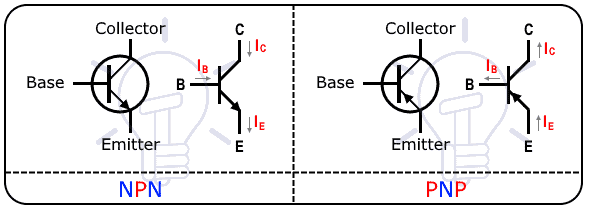
The symbol of the NPN transistor also is used to identify the direction of the current. The little arrowhead pointing outwards of the emitter shows the current direction going outward of the emitter.
As the majority of charge carriers in the collector and emitter are the electrons and they are responsible for the flow of current. Therefore, the majority charge carrier in the NPN transistor is electrons while the minority carrier holes.
NPN transistor switches ON by applying a positive voltage at the base terminal while switches off by applying low voltage 0v at the base terminal.
Since the majority charge carriers are electrons and they are fast, the recovery time of the NPN transistor is fast. It leads to the NPN having a very small switch ON and Switch OFF time, therefore offering a very high switching speed.
Related Posts:
- Difference Between DIAC and TRIAC
- Thyristor and Silicon Controlled Rectifier (SCR) – Thyristors Applications
PNP Transistor
The PNP Transistor is formed by the combination of 2 P-Type layers and 1 N-Type layer. The thin N-layer is sandwiched between two thick P-layers. The middle N-layer is called base while the other two layers are called collector and emitter.
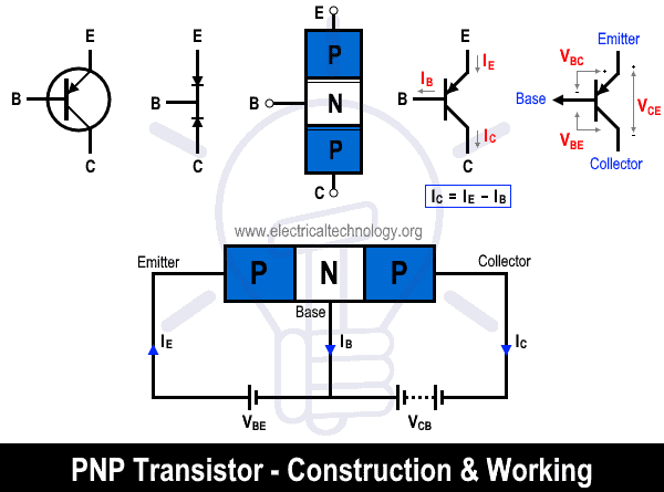 The Collector and emitter have holes as majority charge carriers while the Base has electrons as the majority charge carrier. The minority charge carriers in the collector and emitter are electrons while in the base are holes.
Applying a negative voltage to the base with respect to the emitter will push holes into the base region. As the base has electrons as majority carriers, the holes will combine with the electrons and cause them to penetrate the depletion region. Consequently, the current from the emitter will start to flow towards the collector. This current is due to the presence of majority charge carrier holes.
PNP transistor switches on when a negative voltage is applied to the base region and switches off when a positive voltage is applied. Since the majority charge carriers are holes, the recovery time of the PNP transistor is comparatively high. Therefore, the PNP transistor has a low switching speed.
The symbol of the PNP transistor is different from NPN. It shows an arrowhead pointing inwards showing the direction of the current flowing inside the emitter towards the collector terminal.
Related Posts:
- Difference Between Microprocessor and Microcontroller
- Difference Between 8085 & 8086 Microprocessor – Comparison
Key Difference between NPN & PNP Transistor
The following comparison table shows some of the key differences between a PNP and NPN transistor.
| NPN Transistor | PNP Transistor |
| It is made of a combination of two N-layers and one P-layer. | It is made up of two P-layers and one N-layer. |
| It is formed by sandwiching P-layer between N-layers. | It is formed by sandwiching N-layer between P-layers. |
| Emitter and collector is connected with N-regions. | Emitter and collector is connected with P-regions. |
| The base terminal is connected with P-region. | The base terminal is connected with N-region. |
| The majority charge carriers are electrons. | The majority charge carriers are holes. |
| The minority charge carriers are holes. | The minority charge carriers are electrons. |
| It starts conduction once electrons enter the base region. | It starts conduction once the holes enter the base region. |
| It switches on by applying a positive base voltage. | It switches on by applying a low base voltage. |
| It switches off by applying a low base voltage. | It switches off by applying a positive base voltage |
| The current flows from collector towards emitter. | The current flows from emitter to collector. |
| The base current goes into the base through the emitter. | The base current goes from the emitter into the base. |
| In the NPN symbol, the emitter arrow is pointing outward. | In the PNP symbol, the emitter arrow is pointing inward. |
| It has a small switching time thus having a high switching speed. | It has a high switching time thus having a low switching speed. |
Related Posts:
- Difference Between CPU and GPU – Comparison
- Difference between Analog and Digital Circuit – Digital vs Analog
Properties & Characteristics of PNP & NPN Transistors
The following different properties differentiate both PNP and NPN transistors having different characteristics and applications.
Construction
NPN transistor is made by sandwiching P-layer between two N-layers.
PNP transistor is made by sandwiching N-layer between two P-layers.
Symbol
The symbol of NPN is indicated by having an arrowhead at the emitter pointing outward. While in PNP transistor the arrowhead is pointing inwards.
Current Flow
In the NPN transistor, the direction of current flow is from the collector towards the emitter while in the PNP transistor, the current is directed from the emitter towards the collector. The current direction is also indicated by their symbol.
Switching
The NPN transistor switch on when a positive voltage of high voltage is applied to the base terminal while the PNP transistor switches ON when a negative or low voltage 0v is applied to the base terminal.
Switching Speed
The NPN transistor turns ON and OFF instantaneously. Therefore, the NPN transistor has higher switching speed as compared to the PNP transistor.
Majority Charge Carriers
The current flow in a transistor depends on the majority charge carrier. Therefore, the majority charge carriers in NPN are electrons while in PNP transistor is Holes.
Base Current
The base current in an NPN transistor flows into the base region while in a PNP transistor the base current flows out of the base region.
Related Posts:
- Difference between Electron Current and Conventional Current
- Difference Between RAM and ROM – Comparison
- Difference Between Synchronous and Asynchronous Transmission
- Difference between Inverter & UPS – Uninterruptible Power Supply
- Difference Between Online UPS and Offline UPS – Which One is Better?
- Bipolar Junction Transistor (BJT) – Formulas and Equations
- Transistor, MOSFET and IGFET Symbols
- How to Check a Transistor by Multimeter (DMM+AVO) – NPN & PNP – 4 Ways