NOR and NAND Implementation – Two Level & Multilevel Implementation
NOR and NAND Implementation – Two Level & Multilevel
Introduction to NOR Gate & Its Implementation
NOR gate is a universal gate which can implement any kind of Boolean logic function.
NOR gate is commercially used because it allows the access to wired logic,which is a logic function formed by connecting the outputs of NOR gates. Wired logic does not consist of a physical gate but the wires behave as a logic function. The other reason for commercial usage of NOR gate is that it can be easily fabricated and has a low fabrication cost. It also shrinks the schematic by decreasing the number of gates, which results in small size, fast speed, and Low power consumption.
As we know a typical Boolean function implementation consists of AND Gate, OR Gate and NOT Gate. To implement a whole Boolean function using NOR gate first, we need to implement these gates using NOR gates.
- Related Article: Exclusive-NOR (XNOR) Digital Logic Gate
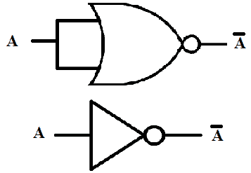
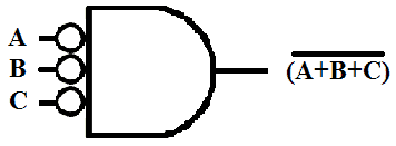
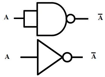
NOT Gate
NOT or Inverter gate complements its input into output. A single input NOR gate also inverts its input. Single input NOR gate means that its inputs are combined into single input line as shown in the figure given below.
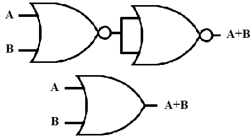
OR Gate
OR logic gate function is complement ( Invert ) of NOR function. So in order to implement OR gate we need two NOR gates. The second NOR gate will be used for complementing the output of the first NOR gate. Schematic of OR gate using NAND gate is given below.
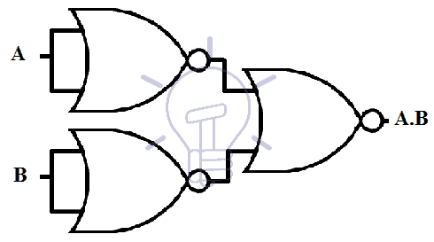
AND Gate
To acquire AND logic gate operation we need three NOR gates. Two NOR gate are used as Inverter to invert the input to the 3rd NOR gate.
According to De Morgan’s law
( A’ + B’ ) = A.B
Schematic of AND gate implementation using NOR gate is given below.
To convert a Boolean circuit with AND, OR and NOT gates into NOR gates, we need to convert the logic function schematic into NOR equivalent schematic. A NOR equivalent schematic contains NOR equivalent gates for every logic gate. These gates need alternate logic symbols. We will discuss these alternate NOR gates one by one.
OR-INVERT
OR-INVERT symbol consists of OR gate symbol with a bubble at the output, which complements the output of OR into NOR.
INVERT-AND
INVERT-AND mean INVERTER connected to the input of AND gate. According to DE Morgan’s law, Inverting the inputs of the AND gate convert it into NOR gate.
( A’.B’.C’ ) = ( A + B + C )’
INVERT-AND symbol is given below.
INVERT-AND symbol consists of AND gate with a bubble at each input for complementation (inversion).
These symbols are used for converting a circuit into NOR gates. When both of these symbols are used in a schematic, it is said to be in mixed notation.
Related Articles
Two-Level Implementation using NOR Gate
Two-level implementation means that any path from input to output contains maximum two gates hence the name two-level for the two levels of gates.
Implementing Two-Level logic using NOR gate requires the Boolean expression to be in Product of Sum (POS) form.
In Product of Sum form, 1st level of the gate is OR gate and 2nd level of the gate is AND gate.
To implement a Boolean function using NOR gate, there are basically three step;
Product of Sum Form
First, you need to have a simplified Product of Sum expression for the function you need to implement.
Simplified Product of Sum expression can be made using Karnaugh Map (K-map) by combining the ‘0’s and then inverting the output function.
Suppose we have simplified POS expression.
F = ( A + B ) ( C + D )
Draw its schematic using AND-OR NOT gates as shown in the figure given below.
Mixed Notation
Next step is to draw the above-mentioned schematic using OR-Invert and Invert-AND gates. OR-Invert should replace OR gates and invert-AND replaces AND gates. This schematic is said to be in mixed notation and its schematic is given below.
A bubble means complement. Two bubbles along a line mean double complementation and they cancel each other. However, a single bubble along a line should be compensated by inserting an Inverter in that line or if it is an input line then you can also feed a complemented input if available.
Related Post:
- Binary Encoder – Construction, Types & Applications
- Binary Decoder – Construction, Types & Applications
NOR Gate Conversion
The last step is to redraw the whole schematic replacing OR-Invert and Invert-AND gate symbol by NOR gate symbol because OR-Invert and Invert-AND are equivalent to NOR gate. The final schematic is shown in the figure given below.
Example of having single bubble in a line:
F = ( A + B ) ( B + C ) D
This function is in simplified Product of Sum form. First, we need to draw its OR-AND schematic.
Now we convert the above-given schematic into mixed notation by converting OR gate into OR-INVERT and AND gate into INVERT-AND.
Input line D to the input of AND gate has a single bubble.To compensate this bubble we need to either insert an inverter in this line or complement the input D if available.
Now replace every OR-Invert and Invert-AND with NOR gate as shown in the figure given below.
Multi-level Implementation using NOR Gate
Schematic having more than two levels of gates is known as a multi-level schematic.
We can implement multi-level POS expression using NOR gate. The conversion of multi-level expression into NOR gate has the same method as two-level implementation.
The multi-level expression can be converted into two-level expression but for the sake of realization, we will implement a multi-level expression.
Suppose a 4-level function:
F = ( A + B ( C + D )) ( B + D’ )
First, we will draw its schematic using AND, OR, NOT gates.

Notice the OR-AND pattern like two-level implementation. It can be easily converted since the bubble cancels each other.
Now we will convert it into mixed notation for NOR.
The two bubbles along a single line cancel each other. However, there is a single bubble at the 2nd level gate’s input. so we will complement the input B to compensate the bubble.
Now redraw the whole schematic replacing OR-Invert and Invert-AND with NOR gate symbol as shown in the figure below.
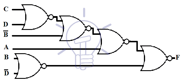
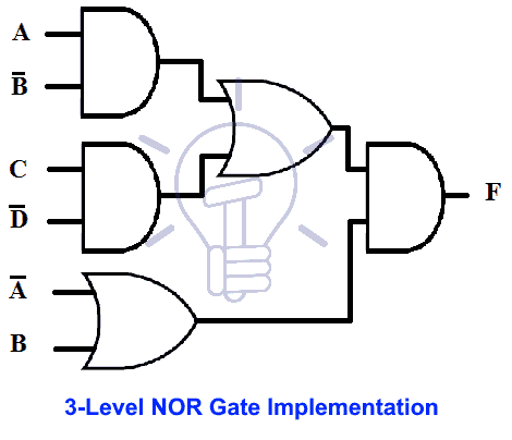
3-Level Implementation & Example using NOR Gate
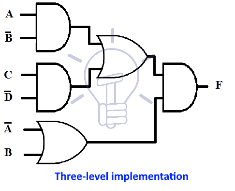
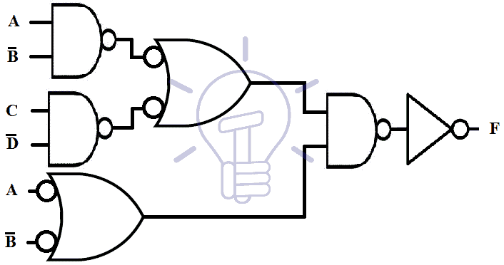
A 3-level implementation using NOR gate’s Example is given below;
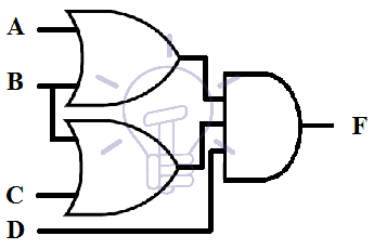
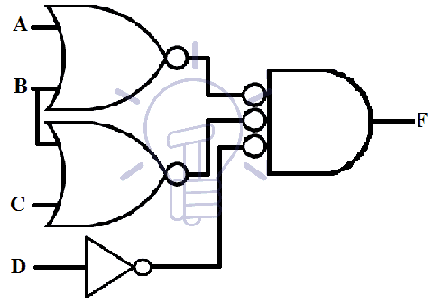
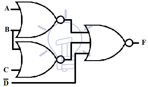
F = ( AB’ + CD’ ) ( A’ + B )
First, we will draw its schematic using AND,OR,NOT gates as given in the figure below.
Now we will convert it into mixed notation for NOR.
The single bubbles at the input line of all first level gates need an inverter or the inputs to be complimented. The two bubbles along the same line cancel each other.
Now that all the bubbles have been accounted for, we will redraw this schematic by replacing OR-Invert and Invert-AND with NOR gates as shown in the figure below.
Introduction to NAND Gate & Its Implementation
NAND Gate is a universal logic gate which means any Boolean logic can be implemented using NAND gate including individual logic gates. In other words, any kind of Boolean function can be implemented using only NAND gates.
NAND gate is commercially used because it allows the access to wired logic which is a logic function formed by connecting the outputs of NAND gates. Wired logic does not consist of a physical gate but the wires behave as a logic function. The other reason for commercial usage of NAND gate is that it can be easily fabricated and has a low fabrication cost. It also shrinks the schematic by decreasing the number of gates, which results in small size and as mall delay, fast speed and Low power consumption.
As we know a typical Boolean function implementation consists of AND, OR and NOT gates. To implement a whole Boolean function using NAND gate first, we need to convert these gates into NAND gate.
Related Articles:
- Digital Asynchronous Counter (Ripple Counter) – Types, Working & Application
- Digital Synchronous Counter – Types, Working & Applications
NOT GATE
NOT gate ( Inverter ) complements its input into the output. A single input NAND gate also complements it input into output. Single input NAND gate means that the inputs of 2-input NAND gates are combined together into a single input line as shown in the figure given below.
AND GATE
NAND gate is negative AND gate. In fact, NAND and AND are inverse to each other. To achieve AND gate operation need two NAND gates. The second NAND gate will be used as an Inverter to complement (Invert) the output of first NAND gate into AND gate.

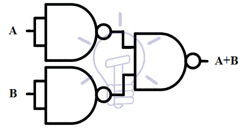
OR GATE
OR gate operation needs three NAND gates. Two NAND gates are used as inverter at the input of the 3rd NAND gate. The two NAND gates invert the input and then the inverted input is fed to the 3rd NAND gate, which results in OR function as shown in figure below;
(A’.B’) = A+B DE Morgan’s law
To convert a Boolean function from NOT, AND, OR gates to NAND gates, we need to convert the schematic into NAND equivalent schematic. NAND equivalent schematic contains NAND equivalent gates. These equivalent gates need alternative symbols to represent; these alternative gates are discussed below;
- BCD to 7-Segment Display Decoder – Construction, Circuit & Operation
-
Binary Multiplier – Types & Binary Multiplication Calculator
AND-INVERT
AND-INVERT means INVERTER (NOT gate) connected to the output of AND gate. As we have discussed before that inverting the output of an AND gate makes it a NAND gate. AND-INVERT symbol represent NAND gate and it is given below;
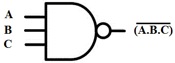
AND-INVERT symbol consists of AND gate followed by small bubble for complementing the output.
INVERT-OR
INVERT-OR means Inverter (NOT gate) connected to the input of OR gate. According to DE Morgan’s law, Inverting the inputs to the OR gate makes it a NAND gate. So INVERT-OR symbol represents NAND gate and it is given in the figure below.
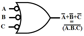
INVERT-OR symbol consists of OR gate with small circles (bubble) at the input for inversion.
These both symbols are used for converting a schematic into NAND gates. When both of these symbols are used in a schematic the circuit is known to be in mixed notation.
Related Articles:
- MUX – Digital Multiplexer | Types, Construction & Applications
- DEMUX – Demultiplexer | Types, Construction & Applications
Two-Level Implementation using NAND Gate
Two-level implementation means that any path from input to output contains maximum two gates hence the name two-level for the two levels of gates.
Implementing a two-level schematic with NAND gates require the expression to be in Sum of Product (SOP) form. In Sum of Product form, the 1st level of the gate is AND gate and the 2nd level of the gate is OR gate. It can be easily converted into NAND gates. To convert any function into two-level NAND schematic there are 3 steps;
Sum of Product Form
First, you need to have simplified Sum of Product (SOP) form for the Boolean function. Karnaugh map (K-map) or Boolean algebraic theorems can be used to get a Simplified SOP expression.
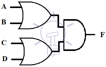
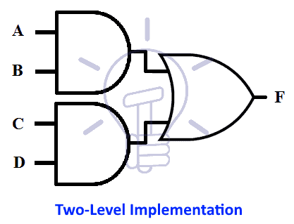
Suppose an SOP function F = A B + C D
This SOP function is in Simplified SOP form and its AND-OR schematic is given below.
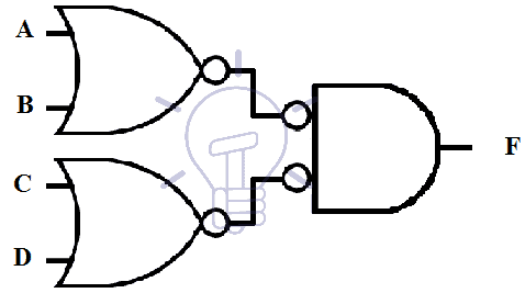
Mixed Notation
2nd step is to convert the AND-OR schematic into mixed notation. In mixed notation for NAND gate, AND gate is converted into AND-invert and OR gate is converted into INVERT-OR. Mixed notation design for the above function is given below.
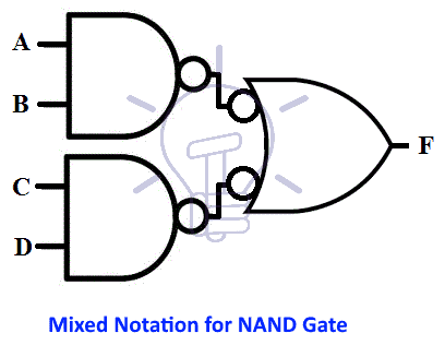
Notice the bubble in a single line. A single bubble means a complement (inversion). Two bubbles on the same line mean double complementation which cancels each other. If there was a single bubble on a line then we have to insert an inverter in that line. We will discuss that in another example.
Also read:
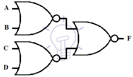
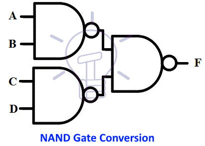
NAND Gate Conversion & Example
The third step is to convert the AND-INVERT and INVERT-OR symbols into its equivalent NAND gate symbol. NAND gate schematic of above function is given below.
Example
Suppose a function F = A B + B C + D to be implemented using NAND gates
This function is in simplified Sum of Product form. First, we need to draw its AND-OR schematic.
Now we convert the above-given schematic into mixed notation by converting AND gate into AND-INVERT and OR gate into INVERT-OR.

Notice the single input D line to the OR gate. There is one bubble on this line. To compensate this bubble we need to either insert an inverter in this line or complement the input D if available. Then convert AND-INVERT and INVERT-OR symbol into NAND symbol as shown in the figure given below;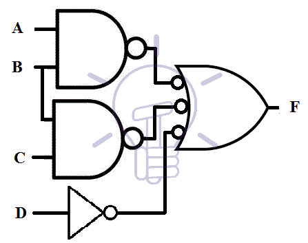
The inverter used here is also a single input NAND gate.
Related Posts:
MULTI-LEVEL Implementation using NAND Gate
Schematic having more than two levels of gates is known as a multi-level schematic.
We can implement multi-level SOP expression using NAND gate. The conversion of multi-level expression into NAND gate has the same method as two-level implementation.
The multi-level expression can be converted into two-level expression but for the sake of realization, we will implement a multi-level expression.
Suppose a multi-level function be;
F = A ( B + CD ) + BD’
This is a four-level function
First, we will draw its AND-OR schematic
Notice the AND-OR pattern. So it can be easily converted into NAND gates. Now we will convert this into mixed notation i.e. AND gate will be converted into AND-INVERT and OR will be converted into INVERT-OR as shown in the figure given below.

Remember double bubbles along a single line cancel each other, and a single bubble along a line should be compensated by inserting an inverter in that line.
Notice the 3rd line of input B, there is a single bubble. To compensate this bubble, either an inverter should be added or the input B should be complimented.
Then redraw the whole schematic using all NAND gates by replacing AND-INVERT and INVERT-OR with NAND gates as shown in the figure below.
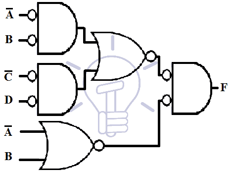
Three-level Implementation & Example using NAND Gate
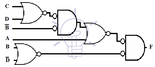
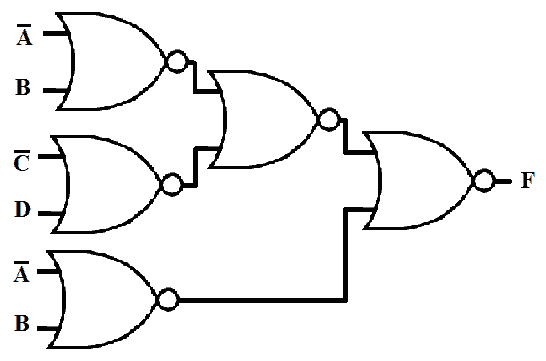
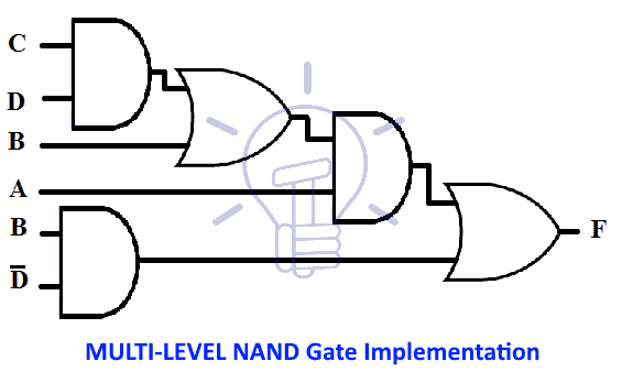
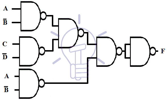
Suppose 3-level function be F = ( AB’+CD’ ) ( A’+B )
First, we will draw its AND-OR schematic as shown in the figure below;
Then we will convert it into Mixed notation by converting AND into AND-INVERT and OR into INVERT-OR.
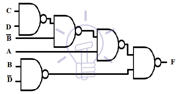
Notice the last two lines with single bubbles. These single bubbles should be compensated by inserting inverters in those lines or complementing the inputs. The output also contains a single bubble so an inverter at the output should also be connected to compensate the bubble.
And the last step is to redraw the whole schematic using all NAND gates instead of AND-INVERT and INVERT-OR as shown in the figure given below.
Related Posts: