MOSFET – Working, Types, Operation, Advantages, and Applications
What is MOSFET? Its Working, Types, Operation, Advantages, Disadvantages & Applications
Transistors are the basic building blocks in electronics and logic circuits where they are used for switching and amplification. MOSFET is a type of FET (Field Effect Transistor) whose gate is electrically isolated by using a insulating layer. Therefore, it is also known as IGFET (Insulated Gate Field Effect Transistor).
What is a MOSFET?
MOSFET or Metal Oxide Semiconductor Field Effect Transistor is a type of FET having four terminals namely Drain, Gate, Source and Body/Substrate. The body terminal is shorted with the source terminal leaving a total of three working terminals just like any other transistor.
The MOSFET conducts current between its source and drain through a path called a channel. The width of this channel is controlled by the voltage at the gate terminal.
MOSFET is a voltage-controlled device whose output depends on the gate voltage. The metal oxide gate is electrically isolated from the channel using a thin layer of silicon dioxide. It increases its input impedance significantly in the range of Megaohms ” 106 = MΩ”. Therefore, MOSFET does not have any input current.
- Related Posts: What is Diode? Construction & Working of PN Junction Diode
Symbol
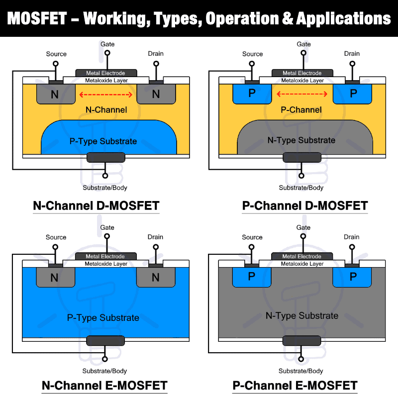
The MOSFET has mainly two types
- Depletion MOSFET or D-MOSFET
- Enhancement MOSFET or E-MOSFET
Both of these types can be divided based on N-channel and P-channel.
 The D-MOSFET is also known as “normally ON” MOSFET because they have a built-in channel is during manufacturing. Applying gate voltage reduces the channel width, switching the MOSFET OFF. While the E-MOSFET is also known as “Normally OFF” MOSFET because there is no channel during fabrication but it is induced by applying voltage.
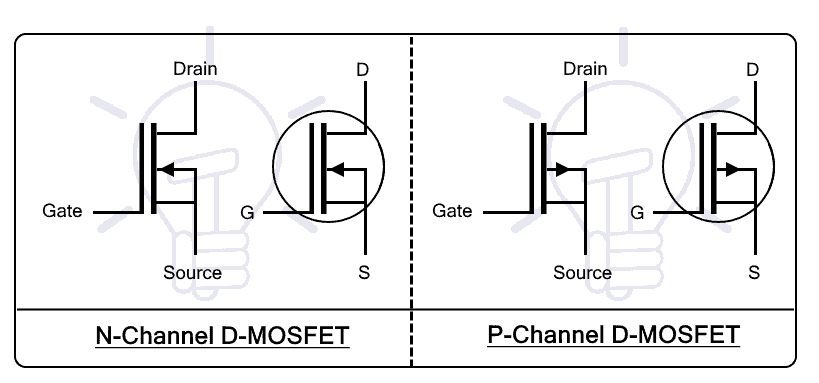
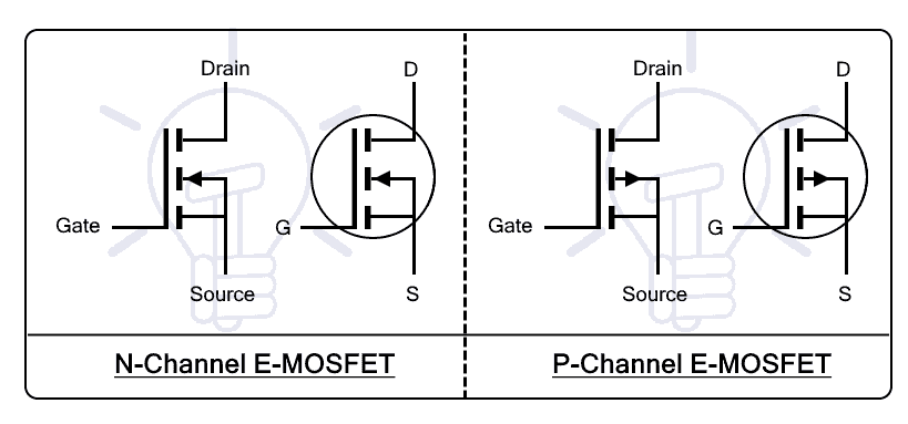
Therefore the D-MOSFET symbol has a continuous line to represent a channel between the drain and source that allows the current flow at zero gate-source voltage. While the broken line in E-MOSFET represents a broken path or absence of channel for current flow at zero gate-source voltage. The arrow pointing inward shows N-channel while the arrow pointing outward show P-channel MOSFET.
MOSFET Regions of Operation
Transistors act like an insulator or a conductor based on a very small signal. The MOSFET just like any other transistor also operates in three regions.
Cutoff Region: In this region, the MOSFET remains turned off and there is no drain current ID. When MOSFET is used as a switch, it utilizes this region as OFF-state or opened-state of a switch.
Saturation Region: In the saturation region, the MOSFET allows a constant current between source and drain. It acts as the ON-state or closed-state of a switch. The MOSFET is fully on allowing maximum drain current ID through it.
Linear or Ohmic Region: In this region, the MOSFET offers constant resistance that is controlled by the voltage level VGS. The drain current ID increases with the level of the voltage VGS. Therefore, this region is used for amplification.
Types of MOSFETs
The MOSFET is classified into two main types:
- Depletion type MOSFET or D-MOSFET – (D & N Channels)
- Enhancement type MOSFET or E-MOSFET – (D & N Channels)
Related Posts:
Depletion MOSFET
The Depletion type MOSFET or D-MOSFET is a type of MOSFET that has a channel constructed during the process of fabrication. In other words, it has a channel even when there is no voltage applied to it. Therefore, it can conduct current between source and drain when the gate-source voltage VGS = 0 volts. Due to this reason, it is also known as “Normally ON” MOSFET.
Connecting the gate-source terminal in reverse bias will deplete the channel of the charge carrier thus the name depletion MOSFET. It reduces the width of the channel until it completely vanishes. At this point, the D-MOSFET stops conduction and this VGS voltage is known as VTH threshold voltage.
If Gate and source is connected in forward bias and the VGS is increased, more majority carriers will get induced in the channel and its width will increase. It will result in increasing the current flow between drain and source. This is why the D-MOSFET can work in both depletion and enhancement mode.
The D-MOSFET can be ‘N-channel D-MOSFET’ or ‘P-channel D-MOSFET’ depending on the channel being used. The type of channel also affects its biasing as well as its speed and current capacities.
- Related Post: Thyristor & Silicon Controlled Rectifier (SCR)
N-Channel D-MOSFET
In N-channel D-MOSFET, the source and drains electrode is placed on small N-type layers. While the gate electrode is placed on top of an insulating metal oxide layer that electrically insulates it from the channel beneath it. The channel made for N-type material is fabricated on top of a P-type substrate.

The channel as it is made of N-type material consists of electrons as charge carriers. The voltage at the gate produces an electric field that affects the flow of these charge carriers.
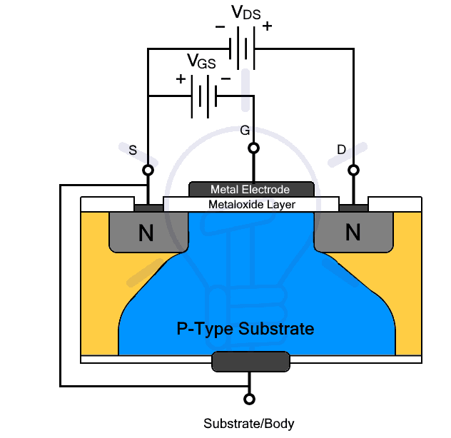
When the gate is connected in reverse bias i.e. negative voltage VGS < 0 volt is applied, the holes from the P-substrate will attract towards the gate, depleting it of the electrons and reduce the channel size. At certain negative VGS the MOSFET will stop conduction as there will be no channel. This VGS is threshold voltage Vth. N-channel MOSFET has –Vth,
While increasing VGS will enhance (increase) its conductivity i.e. the drain current ID will increase with the drain-source voltage VDS. However, this works in the ohmic region. When the VDS reaches the pinch-off voltage Vp, the IDS become saturated IDSS and the current stops increasing. This mode is used for switching applications.
Operating Regions of N-Channel D-MOSFET
Cutoff Region: In this region, the gate-source voltage VGS ≤ -Vth. There is no drain current ID = 0 regardless of the value of VDS. The MOSFET is switched off.
Saturation Region: In this region, the VGS > -Vth and the VDS > Vp . The MOSFET allows maximum drains current IDSS which depends on the VGS.
Linear or Ohmic Region: In this region, VGS > -Vth and the VDS < Vp. the MOSFET acts as an amplifier. In this region, the current ID increases with the VDS while its amplification depends on the VGS as shown in the VI characteristics.
P-Channel D-MOSFET
The P-channel D-MOSFET has the same construction as an N-channel except for the drain, source electrodes lie on P-type layers. and the channel is made of P-layer over an N-type substrate. The charge carriers used are holes. The holes have one disadvantage over electrons. They are quite heavier than electrons and therefore can cause it to lose some speed in operation.
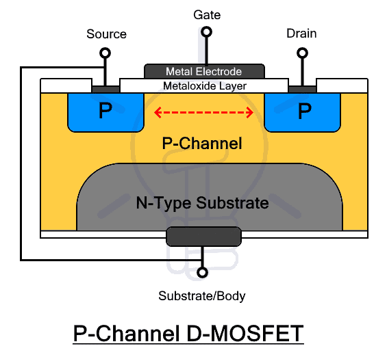
Under normal conditions, it can conduct current between its source and drain as long as there is a voltage between them. the gate voltage can affect the channel width to increase or decrease it.

When a positive VGS is applied at its gate, the electric field will cause to attract the electrons from the N-type substrate that combines with the holes thus depleting the channel of charge carriers. It reduces the width of the channel and the amount of current. at a certain point, the VGS completely eliminates the channel and stops the flow of current.
Therefore, P-channel D-MOSFET has a positive threshold voltage i.e. it switches off when positive VGS is applied and switches on when there is no VGS. Applying negative voltage will induce more holes into the channel causing it to increase or enhance its current conduction.
Related Posts:
- PNP Transistor – Construction, Working & Applications
- NPN Transistor – Construction, Working & Applications
Operating Regions of P-Channel D-MOSFET
Cutoff Region: In this region, the gate-source voltage VGS = +Vth. There is no drain current ID = 0 regardless of the value of VDS. The MOSFET is switched off.
Saturation Region: In this region, the VGS < +Vth and the VDS > Vp. The MOSFET allows maximum drains current IDSS which depends on the level of VGS.
Linear or Ohmic Region: In this region, VGS < +Vth and the VDS < Vp. the MOSFET acts as an amplifier. In this region, the current ID increases with the VDS while its amplification depends on the VGS as shown in the VI characteristics.
Enhancement MOSFET
Enhancement MOSFET or E-MOSFET is a type of MOSFET that does not have a channel during its fabrication. Instead, the channel is induced in the substrate by applying the voltage through its gate electrode. The voltage enhances its conduction ability hence the name.
The E-MOSFET does not conduct and remains switched OFF when there is no voltage at its gate. It is why it is also known as “Normally OFF” MOSFET. By applying a forward voltage between the gate and source, charge carriers are induced in the substrate that produces a channel for the conduction of current between the source and drain.
Applying voltage above threshold voltage enhances the width of the channel and increases the current flow therefore it is named enhancement MOSFET.
The E-MOSFET is also divided into N-Channel and P-Channel E-MOSFET.
N-Channel E-MOSFET
The N-Channel E-MOSFET has the same structure as D-MOSFET except there is no channel during manufacturing. The channel is induced by the application of a voltage across its gate.

N-channel E-MOSFET will not conduct current between its source and drain terminal when the VGS = 0 volts. Because there is no channel to allow current flow. Applying a positive voltage +VGS to the gate produces an electric field beneath the gate layer. It results in attracting the electrons from the P-substrate and pushing back holes away from the insulating layer. A channel in induced which allows the current between the source and drain.

The VGS at which the channel is induced is called Vth threshold voltage and increasing the voltage above Vth causes to enhance the channel width.
- Related Posts: What is Inverter? Types of Inverters and their Applications
Operating Regions of N-Channel E-MOSFET
Cutoff Region: In this region, the gate-source voltage VGS ≤ 0v. There is no drain current ID = 0 regardless of the value of VDS. It operates as a switch.
Saturation Region: In this region, the VGS > 0v and the VDS > VGS. The MOSFET allows maximum drains current IDSS which depends on the level of VGS.
Linear or Ohmic Region: In this region, VGS > 0 and the VDS < VGS. the MOSFET acts as an amplifier. In this region, the current ID increases with the VDS while its amplification depends on the VGS as shown in the VI characteristics.
P-Channel E-MOSFET
P-channel E-MOSFET has the same structure as P-channel D-MOSFET except for the absence of channel. There is no channel during its construction. It is induced by applying VGS.
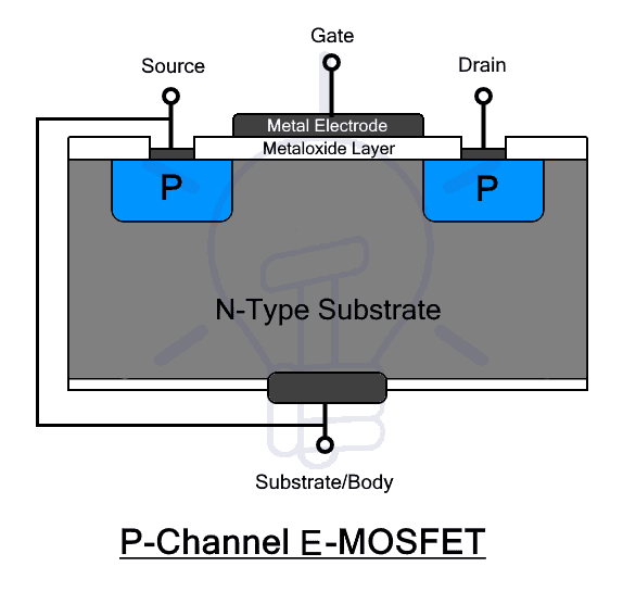
When –VGS is applied to the gate, positive charges (holes) gather beneath the insulating layer and the electrons are pushed back. The holes accumulate together to form a channel between the source and drain. Now, if the voltage between source and drain is applied, it will start to conduct current.
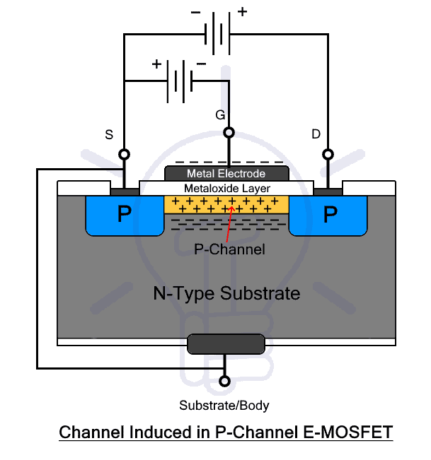
Same as N-channel, it does not conduct when the VGS = 0 V. reducing the voltage below Vth, the channel width increases, allowing more current to flow through it.
Related Posts:
- Seven Segment Display: 7-Segment Display Types, Working & Applications
- What is Filter and Types of Filters with Applications
Operating Regions of N-Channel E-MOSFET
Cutoff Region: In this region, the gate-source voltage VGS ≥ 0v. There is no drain current ID = 0 regardless of the value of VDS. It operates as a switch.
Saturation Region: In this region, the VGS < 0v and the VDS > VGS. The MOSFET allows maximum drains current IDSS which depends on the level of VGS.
Linear or Ohmic Region: In this region, VGS < 0 and the VDS < VGS. The MOSFET acts as an amplifier. In this region, the current ID increases with the VDS while its amplification depends on the VGS as shown in the VI characteristics.
Working of MOSFET
MOSFET can operate like a switch or an amplifier. The operation of a MOSFET depends on its type and its biasing. They can operate in depletion mode or enhancement mode.
MOSFETs have an insulating layer between the channel and the gate electrode. This insulating layer increases its input impedance. Therefore, it does not allow any gate current. Instead, it operates on the voltage applied to its gate terminal.
The insulating layer forms a flat capacitor that has advantages and disadvantages. It creates a very high input impedance and therefore, has very low power consumption. But an electrostatic charge can permanently damage this thin insulating layer.
In depletion mode, MOSFET has a built-in channel between the source and drain terminal. Applying a voltage VDS between the source and drain causes the drain current ID to flow. To reduce or stop the conduction of current ID, the reverse bias voltage VGS is applied to the gate. it depletes the channel of charge carriers, reducing it width.
In Enhancement mode, a forward bias voltage VGS is applied to the gate which attracts the minority charge carriers from the substrate. They accumulate beneath the gate electrode to increase or enhance the width of the channel. This width depends on the amount of gate voltage. Higher the voltage, higher the amount of charge accumulates and wider the channel. Therefore, the drain current ID also increases.
The following table shows the status of all four types of MOSFET at different levels of Gate-Source voltage VGS
| MOSFET Type | VGS = +ve | VGS = 0 | VGS = -ve |
|
N-Channel D-MOSFET |
ON | ON | OFF |
| P-Channel
D-MOSFET |
OFF | ON | ON |
| N-Channel
E-MOSFET |
ON | OFF | OFF |
| P-Channel
E-MOSFET |
OFF | OFF | ON |
The following table shows the operating region of all four MOSFETs.
| MOSFET Type | Cutoff Region
(OFF-State) |
Linear/Ohmic Region
(Amplifier) |
Saturation Region
(ON-State) |
| N-Channel
D-MOSFET |
VGS ≤ -Vth
VDS = …. |
VGS > -Vth
VDS < VP |
VGS > -Vth
VDS ≥ VP |
| P-Channel
D-MOSFET |
VGS ≥ +Vth
VDS = …. |
VGS < -Vth
VDS < VP |
VGS < -Vth
VDS ≥ VP |
| N-Channel
E-MOSFET |
VGS ≤ +Vth
VDS = …. |
VGS > +Vth
VDS < VGS |
VGS > +Vth
VDS ≥ VGS |
| P-Channel
E-MOSFET |
VGS ≥ -Vth
VDS = …. |
VGS < -Vth
VDS < VGS |
VGS < -Vth
VDS ≥ VGS |
VGS Gate to Source Voltage VDS Drain to Source Voltage
Vth Threshold Voltage VP Pinch off Voltage
The Depletion MOSFETs can work in both depletion-mode and enhancement-mode while the Enhancement MOSFET can only work in Enhancement mode.
In FETs, since the drain and source are made from same material, they are interchangeable. The drain is the terminal whose voltage is more positive than the source.
Related Posts:
Characteristics or V-I Curve of MOSFETs
Transfer Characteristics: The transfer characteristics curve shows the relationship between the input gate voltage VGS and the output drain current ID.
Drain Characteristics: The drain characteristics curve shows the relation between the drain-source voltage VDS and drain current ID.
N-Channel D-MOSFET
The N-channel D-MOSFET transfer curve shows that the MOSFET conducts drain current ID when the VGS exceeds above the VTh threshold voltage. The threshold voltage is below 0v which means that it can conduct at 0 VGS.
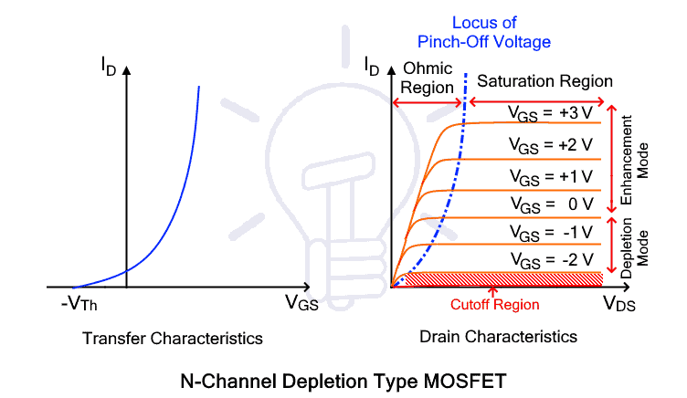
The drain characteristic shows the three operating regions of the MOSFET; cutoff, ohmic and saturation region including both modes of operations i.e. depletion and enhancement mode. The ohmic and saturation regions are separated by a boundary line called locus of pinch-off. The pinch-off voltage is the minimum voltage at which saturation occurs.
In the ohmic region, the drain current ID increases with the VDS . In saturation region, the ID becomes constant called saturation current and only varies with the level of the VGS. In cutoff region, the ID remains zero but the VGS must be brought down below –VTh shown by the transfer curve.
At VGS = 0V or below, the MOSFET operates in depletion mode where the channel width and conductivity reduces with the drop in voltage. While above 0V, it starts to enhance and increase conductivity.
P-Channel D-MOSFET
The negative curve of transfer characteristics shows that P-channel D-MOSFET switches on when the VGS is below the +Vth limit. The drain characteristic curve shows the relation between VDS and ID for different values of VGS. As the gate-source voltage VGS decreases, the current ID starts to increase.

There is not much of a difference between N-channel and p-channel MOSFET except the voltages are reversed.
- Related Post: What is Solid State Relay (SSR)? Types of SSR Relays
N-Channel E-MOSFET
E-MOSFET does not conduct at 0 VGS due to the absence of a channel as shown in the graph. However, once the VGS exceeds threshold voltage Vth, it starts conduction. It has the same operation as a D-MOSFET operating in Enhancement mode.
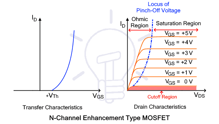
At VGS < VTh, the MOSFET operates in the cutoff region where there is no drain current ID. As the VGS increase above VTh, the ID starts to increases with VDS in the ohmic region. When the VDS cross pinch-off voltage VP, determined by the locus of pinch-off, the ID saturates and becomes constant.
P-Channel E-MOSFET
The P-channel E-MOSFET has the same characteristics curve as the N-channel E-MOSFET except the voltages are reversed.

- Related Posts:
- Types of Counters
- Types of Sensors
Advantages & Disadvantages of MOSFET’s
Advantages
- The main advantage of MOSFET is that there is no gate current i.e. it does not have any input current.
- It has a very high input impedance due to the insulation layer.
- It consumes negligible energy in its operation due to a very low leakage current.
- It has a very high switching speed.
- It is used for very high-frequency applications.
- It has very low output resistance.
- It has very small size.
- They can operate at either depletion mode or enhancement mode.
- It provides greater efficiency while operating at low voltages.
- It is unipolar having a noiseless operation.
- It is a voltage-controlled device with very low power loss.
Disadvantages
- Due to insulating layer, there is a capacitance between the gate and channel which can get damaged due to any electrostatic charge buildup.
- It cannot handle high voltages.
- MOSFETs are expensive than BJTs
Related Posts:
Applications of MOSFETs
MOSFET are mainly used for switching and amplification in electronic circuits. Following are some of the applications of MOSFETs.
- It is used for fast switching and amplification of very small signals such as in high frequency amplifiers.
- Power MOSFETs are used for power regulation in DC motors.
- MOSFET are best for chopper circuits due to its high switching speed.
- Due to their high efficiency and low power consumption, they are used for their superior switching speed in digital IC (integrated circuits) such as microcontroller and microprocessors.
- They are used in SMPS (Switch Mode Power Supply)
- They are used in CMOS (Complementary Metal Oxide Semiconductor) logic circuit where the layers of P-MOS and N-MOS are combined together to reduce the space and power consumption.
- They are used in H-bridge circuit.
- They are also used in buck converters and boost converters.
Related Posts:
- What is Resistor and Types of Resistors?
- What is Capacitor and Types of Capacitors?
- What is Inductor and Types of Inductors?
- Digital to Analog Converter (DAC) – Types, Working & Applications
- Analog to Digital Converter (ADC) – Block Diagram, Factors & Applications
- What is Microprocessor and Types of Microprocessors?
- What is Microcontroller and Types of Microcontrollers?


very super explaination 🙏🙏🙏❤️❤️