Electronic Circuit Breaker – Schematic and Working
Electronic Circuit Breaker – Circuit Diagram, Working and Applications
AC device that we use in our homes generally have a limit to handle the current and voltage. These threshold voltage and current are called the device rating, and are the measurements given by the manufacturers in the range of which the device will work properly. Not only are the rated voltage and current required for the most optimum operation conditions, they are also the measurements above which the device may get damaged. The faulty device sometimes harms other devices which are connected to the same network.
This problems occur due to the fluctuations in the voltage which we get from our power grid and are generally inevitable. These voltages surges are responsible for damaging many electronic devices ranging from small electronic appliances in our homes to large high performance industrial machines. The article deals with how to make an electronic circuit breaker which would use its circuitry in a way to save our devices from sudden voltage surges and disconnects the load from the network.
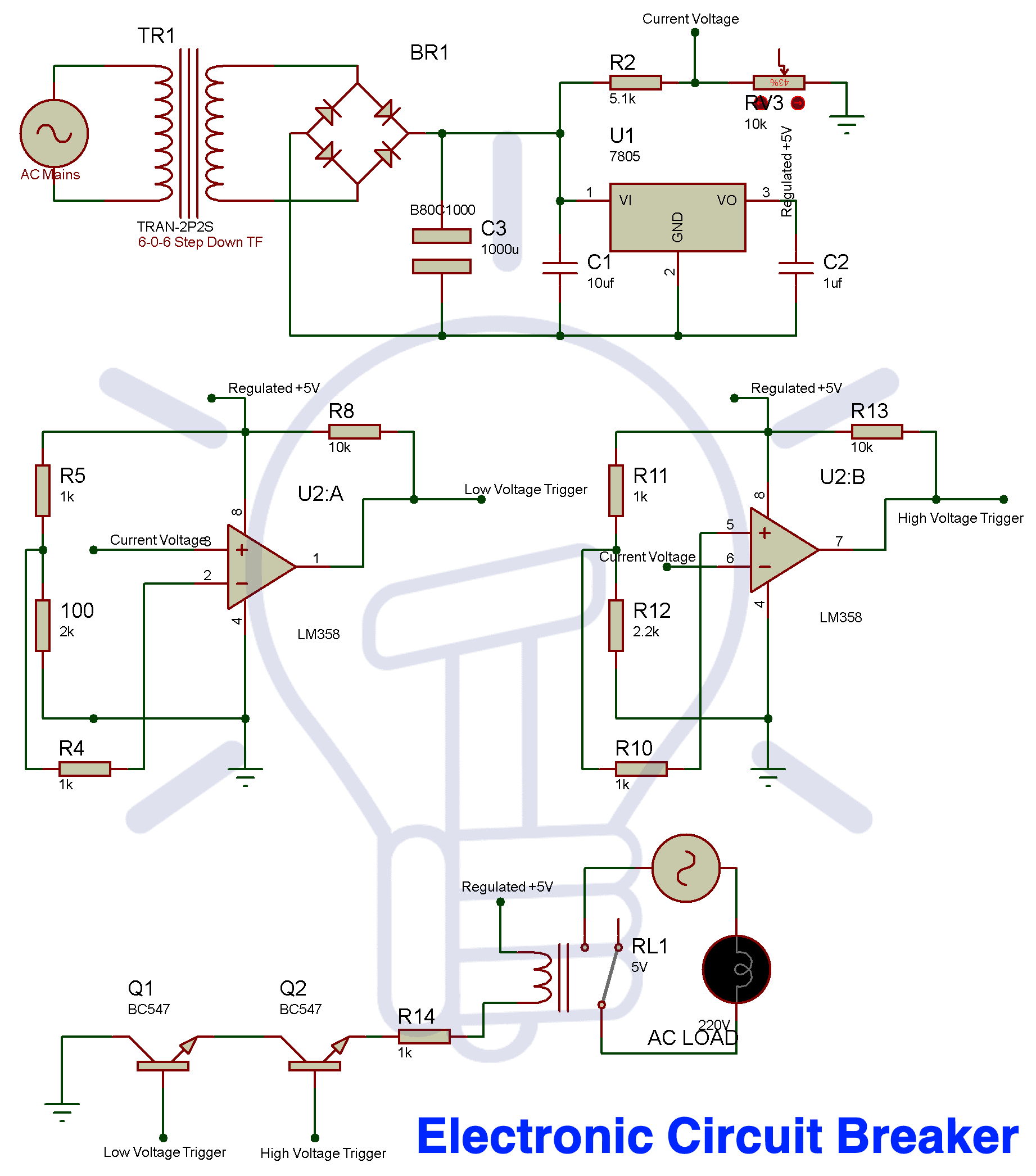
Circuit Diagram of Electronic Circuit Breaker
A schematic diagram of the circuit is given below:
Components Required for Electronic CB
- LM358 Op-Amp
- 7805 Regulator = +5V
- Relay = 5V
- BC547 ICs = 2 Nos
- Step-down Transformer = 12V
- Variable Potentiometer = 10kΩ
- Diode bridge
- Resistors = 1kΩ, 2kΩ, 2.2kΩ, 5.1kΩ & 10kΩ
- Capacitors = 0.1μF, 10μF & 100μF
LM358
The LM358 IC is an Op-Amp IC. It is a low power dual channel Op-Amp IC. It has two internally frequency compensated, independent, high gain Op-Amp. It is made so that it works off of a single power supply and can operate over a wide range of voltages. There are many applications of this IC which include the DC gain block, transducer amplifiers and the conventional Op-Amp circuits. This IC has eight pins package.
The pin out is shown in the figure below.

The internal structure of the IC is shown in the figure above. The IC as discussed above has two independent Op-Amps. The terminals 1 and 7 are the output terminals of the Op-Amp. The terminals 3 and 5 are the non-inverting terminals whereas the terminals 2 and 6 are the inverting terminals. There are the normally present ground and VCC terminals at 4 and 8 respectively.
This IC along with being economical and easily available has some more redeeming features of itself that are more towards the electronic side of it. Some of the features of listed below.
- Its main selling point, the two Op-Amps are internally frequency compensated
- The range of single power supply is 3-32 V.
- The range of dual power supply is -16 to -1.5V or from 1.5V to 16V.
- Voltage gain is 100dB and the bandwidth is 1 MHz.
- Supply current drain to the IC is very low. It is generally in the range of 500µA.
- There is a small offset voltage at the input, which is generally about 2mV.
- Common mode voltage obtained from the IC contains the ground potential.
- The differential input voltage and the power supply voltage given to the IC is comparable.
Related Post: Simple Overvoltage Protection Circuit using Zener Diode
7805 Regulator IC
Circuits that have voltage sources in them may have fluctuations resulting in not providing a fixed voltage outputs. One of the popular ICs for this purpose is 7805 Regulator IC, which is a member of fixed linear voltage regulators used to maintain such fluctuations. There are many application in which the 7805 is used and the major ones are:
- Fixed-output regulator
- Positive regulator in negative
- Adjustable output regulator
- Current regulator
- Adjustable DC voltage regulator
- Regulated dual supply
- Output polarity reversal protection circuit
- Reverse bias projection circuit
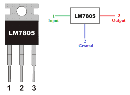
| LM 7805 Voltage Regulator IC | ||
| Pin no | Pin name | Purpose |
| 1 | Input | Apply an unregulated voltage to get a regulated output |
| 2 | Ground | Connected to ground |
| 3 | Output | Output is a regulated voltage signal |
The IC when given an input voltage of 7.2V, will achieve its maximum efficiency.
In IC 7805 voltage regulator, lots of energy is exhausted in the form of the heat. The difference in the value of the input voltage and the output voltage comes as heat. So, if the difference between input voltage and output voltage is high, there will be more heat generation. The hole in the transistor is for connecting a heat sink with it. Therefore, this IC also provides a provision for a heat sink.
Related Post: Automatic Doorbell with Object Detection By Arduino
BC547 Transistor
BC547 is an NPN bipolar junction transistor. Mostly it is used for the switching purpose as well as for amplification processes. The smaller amount of current at the base is used to control the larger amount of currents at collector and emitter as well. Its basic applications are switching and amplification. Below is the pinout of the BC547 transistor:

The working of the transistor is straightforward. When the input voltage is applied at its terminals, some amount of current starts to flow from base to the emitter and controls the current at collector. The voltage between the base and the emitter is negative at the emitter and positive at the base terminal for its NPN construction.
Related Post: Cable and Wire Tester Circuit Diagram
Relay
A relay is an electrically, electromagnetically or electronically operated switch. The switch may have any number of contacts in multiple contact forms, such as make contacts, break contacts, or combination of these two. Relays are used to control a circuit by an independent low-power signal, or where several circuits must be controlled by one signal. The traditional form of relays uses an electromagnet to close or open the contacts, but other operating principles have been invented, such as in solid state relay which use semiconductor properties for control without relying on any moving parts. The pinout of a 5V relay which is used in the circuit’s construction is given below.

| 5V Relay | ||
| Pin no | Pin name | Description |
| 1 | Coil end 1 | Used to trigger the relay |
| 2 | Coil end 2 | Used to trigger the relay |
| 3 | Common(COM) | Connected to one end of the load |
| 4 | Normally close (NC) | If the other end is connected to this terminal, the load remains connected before trigger |
| 5 | Normally open(NO) | If the other end is connected to this terminal, the load remains disconnected before trigger |
Related Post: Smart Home Automation System – Circuit and Source Code
Working of Electronic Circuit Breaker
Connect the components correctly according to the circuit diagram above.The circuit diagram that is shown above has three parts to it. The three parts are to be connected to form a single big circuit. The three parts are
- Power Module
- Op-Amp Module
- Relay Module
The three modules of the circuit will be discussed in brief in the upcoming section of the report.
Power Module
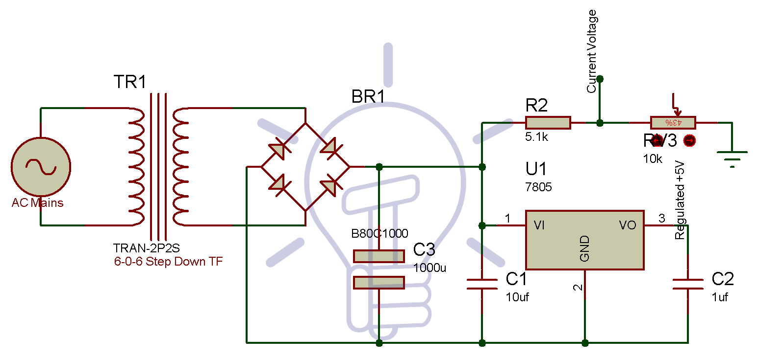
The Op-Amp in this circuit is the controller for the circuit breaker for our project. This Op-Amp requires a 5V regulated power supply. We will be running this circuit off of our mains which has an AC voltage of about 220V. First to power the Op-Amp we need to step down the voltage that is available to us from mains.
For this we use a step-down transformer, in our case we used a transformer which gives us a stepped down voltage of 12V. This 12V AV voltage which is obtained from the transformer is then rectified using a rectifier circuit made using diode bridge. This rectifies the AC voltage to DC voltage.
The output of this rectification will now give us approximately 12V DC voltage. This 12V DC is then regulated using our LM7805 voltage regulator IC. We can map the output voltage of the power module anywhere between 0 to 5V by using a potential divider with a variable resistance and a resistor. By changing potentiometer voltage, we can get different voltages. You may use the 12V to 5V converter circuit as well.
Related Post: Soldering Iron Temperature Controller
Op-amp Module

The Op-Amp module is the main portion of the circuit, and this is where the comparison of voltages take place. Because the circuit breaker we are making is one which provides protection from both high and low voltage surges, we have to take into consideration both the cases. Both the cases have their individual circuit and connect to the main circuit at the labelled connection.
The Op-Amp in the circuit is used in differential mode. And of all the applications of an Op-Amp, we have used the Op-Amp in this circuit as a voltage comparator. This comparator will give either high or low as the output after comparing voltages at two of its terminals. We can set the threshold voltages for both the lower limit and the upper limit can be set using resistor networks.
Related Post: Electronic Eye Circuit – Using LDR and IC 4049 For Security Control
Relay Module

Now that we have given the proper power supply to the Op-Amp circuit and the Op-Amps are made to function the way they are supposed to, we now have to think about the working of the circuit after a detection of high or low voltage surge is identified by the electronic circuit breaker.
The surge of voltage is obtained from the Op-Amp module of the circuit, which is discussed above. Based on the Op-Amps output obtained from the Op-Amp module, the relay will be triggered. When both the outputs from the Op-Amps are high, only then the relay will be triggered and the AC load is directly connected to the mains. There is an additional 1k ohm resistor that is used for current limiting.
Related Projects:
- Electronics Final Year Projects Ideas List
- Electronics Engineering Project Ideas for Engineering Students
- Simple and Basic Electronics Mini Project Ideas for Beginners
- Top Electrical Mini Projects Ideas List
- Electrical Engineering Final Year Projects
- Top Electrical Projects ideas for Engineering Students


The Relay will never be energised. The transistors Q1 and Q2 have been configured with their collector and emitter interchanged in the design. Please correct the schematic.
I was wondering about the same thing, transistors wired incorrectly
Good⭐⭐⭐
I failed to see the advantage of a WiFi circuit breaker – to know it was activated I don’t need a WiFi message, I can see the lights going out … what’s the big deal ???
Good and simple design. Thanks