Difference Between BJT and FET Transistors
What are the Main Differences Between BJT and FET Transistor?
A transistor is a semiconductor device that is used for switching and amplification. BJT and FET are two different types of transistors. Apart from being transistors and both able to do switching as well as amplification, they are quite different from each other. For instance, BJT is a current-controlled current device while FET is a voltage-controlled current device. There are several other differences between BJT and FET.
Related Posts:
- Difference Between Diode and Transistor
- What is The Difference Between Transistor and Thyristor (SCR)?
Before going into the list of differences between BJT and FET, we are going to discuss the basics of BJT and FET.
BJT (Bipolar Junction Transistor)
BJT stands for Bipolar Junction Transistor. These types of transistors are bipolar means that the current flow is due to two types of charge carriers i.e. electrons and holes. There are two types of BJTs i.e. NPN and PNP transistor. They are used for switching as well as amplification of a small signal.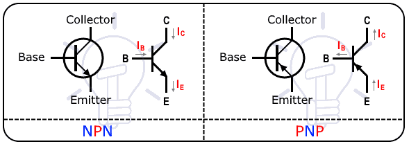
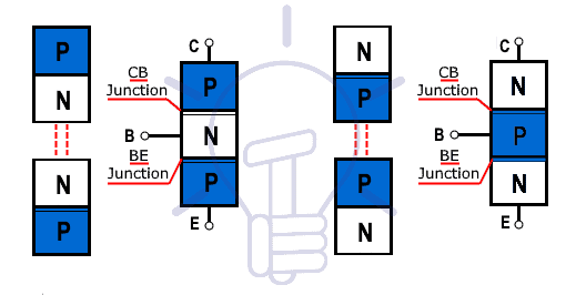
A BJT is made of three alternating layers of P-type and N-type semiconductor materials. NPN is made by sandwiching P-layer between two N-layers while PNP is made by sandwiching N-layer between two P-layers. Since there are three alternating layers, there are 2 PN junctions in a BJT transistor, thus the name junction transistor
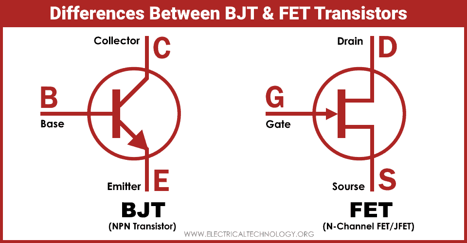
The three terminals of BJT transistors are named Emitter, Base and Collector. Each terminal is connected with each layer of the transistor. The base is the middle layer that is the most lightly doped layer of all. The emitter and collector are both heavily doped with the emitter comparatively heavily doped than the collector.
By connecting the base-collector junction in reverse and base-emitter junction in forward bias allows the flow of current. Based on the type of BJT, current entering through the base allows a current between the collector and emitter which is proportional to the base current. Therefore, BJT is also known as a current-controlled current device.
BJT can operate in 3 regions i.e. Active, Saturated and cutoff region. In the active region, it acts as an amplifier where the collector current is proportional to the base current. while in the saturated and cutoff region, it acts as a switch to make or break a connection.
Since the input (base) is forward biased, the input impedance of a BJT is very low in the range of 1K ohm while the output impedance is very high. Therefore, the gain of the BJT amplifier is very high as compared to FET.
Since the current flow is due to electrons as well as holes, the recovery time i.e. the time it takes to switch off and switch on is large as compared to FET. Therefore, the BJT has a low switching speed as compared to FET. BJT is not suitable for very high frequency.
BJT works if there is any base current i.e. it is controlled by the current flow at its base terminal. Therefore, it consumes energy while operating. Due to this, the BJT consumes more power which is wasted in the form of heat.
Therefore, BJT gets hot very quickly and the temperature also affects its operation. This is why its temperature must be regulated using large heatsinks in order to work normally. BJT is temperature-dependent
Related Posts:
FET (Field Effect Transistor)
FET stands for the Field-Effect Transistor. The current flow in FET is due to the flow of only one type of charge carrier i.e. either electrons or holes. Therefore, FET is also known as a unipolar transistor. There are two types of FET transistors i.e. JFET (Junction FET) and MOSFET (Metal Oxide Semiconductor FET). These transistors are also used for switching as well as amplification in electronic circuits.
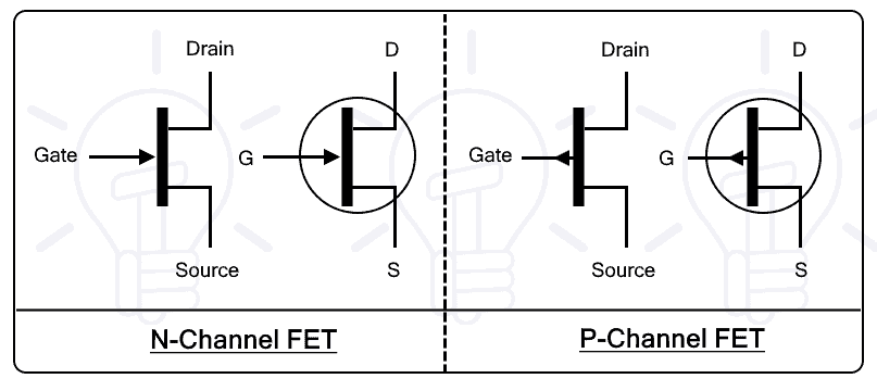 The three terminals of FET are Drain, Gate and source. Based on its construction, FET is available in two types i.e. N-channel FET or P-channel FET. The channel refers to the path for the flow of current from source to drain terminal. The carriers enter the channel through the source and leave out at the drain. There are no PN junctions between the source and drain. The Gate region is made from alternate material as compared to the channel.
 The Gate is reversed biased in order to form a depletion region so that the channel between drain and source is formed. Which leads to the current flow. Increasing the reverse bias voltage at the gate increases the depletion region which results in increasing the current flow. Therefore, the voltage at the gate is used to control the output current. Therefore FET is also known as a voltage-controlled current device.
 There is very little difference between the source and drain terminal. The drain terminal should be connected to a more positive voltage as compared to the source terminal. Therefore, they can be swapped i.e. the drain and the source terminal can be interchanged by maintaining the more positive voltage at the drain terminal.
The majority charge carrier is identified by the type of FET being used. N-channel FET uses electrons for charge carrier while P-channel FET uses holes for charge carrier.
.FET has 3 regions i.e. Active, saturated and cutoff region. The FET acts as an amplifier in the active region while it acts as a switch in the saturated and cutoff regions.
Since the input (gate) is reversed biased, the input impedance of FET is very high in the range of 100M ohm which is why there is no current flow at the gate terminal. And the output impedance is low. Therefore FET does not have a very high gain as compared to BJT.
Since the FET utilize only one type of charge carrier either electrons or holes, the recovery time is very fast. Therefore, its switching speed is very fast and it can be used for very high-frequency applications.
FET does not have any current flow at its base or it is very negligible. Due to which there is no energy consumption during operation. Therefore, FET consumes very low power and is more energy efficient.
Related Posts:
- Bipolar Junction Transistor (BJT) | Construction, Working, Types & Applications
- Thyristor and Silicon Controlled Rectifier (SCR) – Thyristors Applications
Key Differences Between BJT and FET
The following comparison table shows the main differences between BJT and FET transistors.
| BJT | FET |
| BJT stands for Bipolar Junction Transistor. | FET stands Field Effect Transistor. |
| The current flow is due to the flow of majority as well as minority charge carriers. | The current flow is due to the flow of majority charge carriers. |
| Current flow is due to both electrons and holes, therefore name bipolar transistor. | The current flow is due to either electrons or holes, therefore, named unipolar transistor. |
| There are two types of BJT i.e. NPN and PNP. | The two types of FET are JFET and MOSFET, each with N-channel and p-channel as well. |
| BJT construction is comparatively easier. | The FET construction is comparatively difficult. |
| The 3 terminals are named emitter, base and collector. | The 3 terminals of FET are Source Gate and Drain. |
| There are 2 PN junction in BJT. | There are no PN junctions. |
| It is a current-controlled current device. | It is a voltage-controlled current device. |
| The B-E junction is forward biased and the B-C junction is reversed biased. | The Gate voltage is reversed biased while the drain voltage is maintained higher than the source. |
| The BJT has very simple biasing. | The FET biasing is a little difficult. |
| The emitter and base cannot be interchanged or swapped. | The drain and source can be interchanged since the drain should be more positive. |
| BJT has a very high gain. | FET has a comparatively low gain. |
| The input impedance is very low in the range of 1K ohms. | The input impedance is very high in the range of 100M ohms. |
| The output impedance is very high thus high gain. | The output impedance is very low thus low gain. |
| There is current flow at its base terminal. | There is negligible current at its base terminal. |
| BJT has an offset voltage requirement. | FET does not require offset voltage. |
| Dependent on input current, It consumes high input energy at normal operation. | Dependent on input voltage, It consumes less energy in normal operation. |
| BJT consume high power thus not energy efficient. | FET consumes less power thus energy efficient. |
| BJT has a comparatively low switching speed. | FET has a comparatively very high switching speed. |
| BJT generates noise in the system. | FET is very noiseless. |
| BJT is cheaper than FET. | FET is costlier than FET. |
| The size of BJT is larger than FET. | The FET has a more compact and smaller size than BJT. |
| BJT has a negative temperature coefficient. | FET has a positive temperature coefficient. |
| Suitable for low input current application. | Suitable for low input voltage application. |
Related Posts:
- Difference Between Microprocessor and Microcontroller
- Difference Between 8085 and 8086 Microprocessor – Comparison
Properties and Characteristics of BJT & FET
The following different properties differentiate both FET and BJT having different characteristics and applications.
Construction
- BJT has a very simple and easier construction made from alternating semiconductor layers.
- Either P-layer or N-layer is sandwiched between two N-layer or P-layers respectively.
- FET has a little complex construction.
- FET has either an N-channel or a P-channel between the gate of the P-layer or the N-layer respectively.
- The channel is used for the flow of majority charge carriers.
PN Junctions
- BJT transistor has two PN junctions between its collector and emitter.
- One PN junction between Collector and Base and the other between Base and Emitter.
- The FET transistor has no PN junction between its drain and source.
Charge Carrier
- The BJT utilize both type of charge carriers for the flow of current.
- During its operation, holes and electrons flow to conduct current.
- The FET utilize only one type of charge carrier for the current flow.
- It either uses holes in P-channel FET or electrons in N-channel FET.
Types
- BJT has two types i.e. PNP and NPN
- FET has two major types i.e. JFET (Junction FET) and MOSFET (Metal Oxide Semiconductor FET)
- Each type of FET is further classified on the basis of channel i.e. N-channel and P-channel.
Related Posts:
- Difference Between CPU and GPU – Comparison
- Difference between Analog and Digital Circuit – Digital vs Analog
Terminals
- The 3 terminals of BJT are named Collector, Base and Emitter.
- Emitter and Collector are made of the same material with emitter having high doping rate.
- The 3 terminals of FET are named Drain, Gate and Source.
- The drain and source are the two ends of the channel made from the same type.
Input and Output
- The BJT is a current controlled device.
- Its input (at the base) is current which controls the output collector current.
- The FET is a voltage-controlled device.
- Its input is a voltage or potential difference (at the gate) which controls the output current at the source.
I/O Impedance
- BJT operates by having a base-emitter (input) junction in forward bias.
- Therefore, their input impedance is low.
- Their output impedance is very high.
- FET operates by having a gate at reverse bias.
- Therefore, its input impedance is very high.
- While its output impedance is very low.
Isolation
- In BJT, the input at the base terminal is not isolated from the output.
- In FET, the input at the gate terminal is in reverse bias and the input is isolated from the output.
Biasing
- In BJT, the B-E junction is in forward bias while the C-B junction is in reverse bias.
- IN FET, Gate is in reverse bias while the drain is at more positive voltage than the collector.
Gain
- The BJT has very high gain due to its very high output impedance.
- The FET has comparatively lower gain due to its low output impedance.
Terminal Swapping
- In BJT, the terminals cannot be interchanged or swapped.
- The emitter and collector are completely different terminals.
- In FET, the drain and source terminal can be swapped.
- The drain will be the terminal having more positive voltage.
Energy Consumption
- The BJT takes current at its base terminal during continuous operation.
- Therefore, it consumes energy and drains the battery.
- The FET operates on the basis of the gate voltage.
- Therefore, it is energy efficient and does not drain the battery.
Switching Speed
- Since BJT use the flow of both type of charge carriers, its recovery time is slow.
- Therefore, its switching speed is slow.
- FET uses only one type of charge carrier having a fast recovery time.
- Therefore, FET has a very fast switching speed.
Noise
- The BJT is noisy and generates noise in the system. Therefore, not suitable for sensitive digital systems.
- The FET is quite noiseless and is perfect for the sensitive system.
Cost
- BJT having very simple construction is very cheap to manufacture.
- FET having complex construction is comparatively costlier.
Size
- The size of BJT is large. Therefore circuit made of BJT is bulkier.
- The FET is more compact and smaller in size. Suitable for compact and small circuits.
Application
- BJT is used for amplification of a very small current having a medium frequency.
- However, the power consumption and size of the circuit should also be considered.
- The FET is preferred for small voltage signals having a very high frequency.
- Although they are costly and biasing is a little difficult.
Related Posts:
- Difference Between Diode and SCR (Thyristor)
- Difference between Electron Current and Conventional Current
- Difference Between RAM and ROM – Comparison
- Difference Between Synchronous and Asynchronous Transmission
- Difference between Inverter and UPS – Uninterruptible Power Supply
- Difference Between Online UPS and Offline UPS – Which One is Better?
- Diode Symbols – Electronic and Electrical Symbols
- Transistor, MOSFET and IGFET Symbols
- How to Check a Transistor by Multimeter (DMM+AVO) – NPN and PNP – 4 Ways
- How to Test a Diode using Digital and Analog Multimeter – 4 Ways.