Basic Voltage Doubler Circuit Diagram using 555 Timer IC
How to Make a Basic Voltage Doubler Circuit?
As the name of the article suggests, today this article is to help design a circuit which at its output gives a voltage that is double of that which is applied at its input. For example, supplying a 10V input to the voltage doubler circuit will give 20V at its output.
This is one of the many circuits that are readily available for voltage conversion, but this is a cheap and more efficient way to double a voltage in contrast to using a transformer that is bulky and sometimes inconvenient for small applications.
These circuits use capacitors to store energy, and are in some form a rectifier circuit. The switching diodes are generally diodes, which help to bring down the cost instead of using a more expensive counterpart for example a MOSFET, or a BJT.
Voltage doubler circuit is a circuit from the family of voltage multiplier circuit. In this article, we are going to learn how to make a voltage doubler circuit using a 555-timer along with other important components and their brief description.
Related Projects:
- Dual Power Supply Circuit Diagram – 230VAC to ±12VDC
- How to Make a Voltage Tripler Circuit?
- 12V to 5V Converter Circuit
Voltage Doubler Circuit Diagram
Connect the components properly in the same way as shown in the figure below.
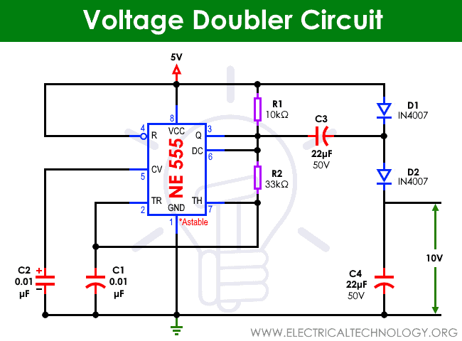
Components Required
- 555-Timer IC
- Diodes – 1N4007
- Resistors – 10kΩ and 33kΩ
- Capacitors – 22μF and 0.01μF
- A power supply
555 Timer IC
The 555 timer IC is an integrated circuit used in a variety of time, pulse generation, and oscillator applications. Introduced in 1972, the 555 Timer IC is still in widespread use due to its very low price and stability. The pin diagram of the 555 Timer IC is given below:
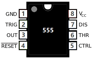
| 555 Timer IC | ||
| Pin no. | Pin Name | Purpose |
| 1 | GND | Ground reference voltage |
| 2 | TRIG | Controls output |
| 3 | OUT | Is driven to ~1.7V below VCC or to ground |
| 4 | RESET | Reset a timing interval |
| 5 | CTRL | Provides access to the internal voltage divider |
| 6 | THR | Acts as the threshold as to when to stop the timing interval |
| 7 | DIS | Open collector output to discharge capacitor |
| 8 | VCC | Positive supply voltage |
There are three modes of operation of the Timer IC, which are bistable, monostable and astable mode.
- In bistable mode, the circuit produces 2-stable state signals that are in low and high states. The output signals of low and high states signals are controlled by reset and activating the input pins.
- In monostable mode, the circuit generates only single pulse when the timer gets an indication from input of the trigger button.
- In astable mode, the circuit of the IC produces a continuous pulse with exact frequency based on the value of the two resistors and capacitors which are connected in the external circuit.
Related Projects:
- Automatic Bathroom Light Switch Circuit Diagram and Operation
- Automatic Doorbell with Object Detection By Arduino
1N4007 Diode
1N4007 is a PN junction rectifier diode. These types of diodes allow only the flow of the electrical current in one direction. 1N4007 has different real life applications, e.g. free-wheeling diodes applications, general purpose rectification of power supplies, inverters, converters etc.
| 1N4007 Diode Pinout | ||
| Pin no. | Pin name | Charge |
| 1 | Anode | +Ve |
| 2 | Cathode | -Ve |
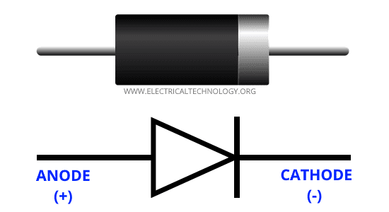
The diagram above shows the symbolic and the actual picture of the 1N4007. The understanding of any component of an electrical circuit is vastly improved when the electrical characteristics of that device is known.
| 1N4007 Electrical Characteristics | ||
| Parameter | Values | Units |
| Forward voltage at 1.0 A | 1.1 | V |
| Reverse current at 25°C | 5 | μA |
| Total capacitance at 1.0 MHz | 15 | pF |
| Maximum full load reverse current at 75° | 30 | μA |
| Average rectified forward current | 1 | A |
| Peak repetitive reverse voltage | 1000 | V |
The diode 1N4007 features are as follows:
- Low leakage current
- Low forward voltage drop
- High forward surge capability
Related Projects:
- How to Make a Simple LED Flashing Circuit using 555 Timer IC
- PCB Design of LED Flasher Circuit using 555 Timer.
This diode has a lot of real life applications in Embedded systems, a few of the major applications associated with the particular diode are given below:
- Converters
- For switching purposes in embedded systems
- Freewheeling diodes applications
- Inverters
- General power rectification of power supplies
- To avoid reverse current and protecting microcontrollers like Arduino or PIC microcontroller.
Working of Voltage Doubler Circuit
As seen in the circuit diagram, the circuit works in two halves that complement each other. The first part of the circuit, which involves the use of the 555 timer, is used in Astable mode, to generate a pulse of square wave.
The second part of the circuit is the one which actually doubles the voltage and consists of 2 capacitors and 2 diodes connected in the manner shown in the circuit diagram. The 555-timer has multiple modes in which we have decided today to use astable Multivibrator mode.
This mode can be used to generate a square wave of approximately 2KHz using a combination of two resistors and a capacitor. From the circuit, we can see that when the pin 3 of the timer IC has a low output, then the diode D1 gets forward biased, which will charge capacitor C3 through it.
Because the capacitor is charged directly from the supply, the capacitor will also get charged to the voltage equal to the input voltage. When the pulse from the timer IC is high, the pin 3 of the IC will show a high output. This will make the diode D1 reversed biased and this blocks the charging of the capacitor C3 which has now been charged to approximately the voltage equal to the supply voltage.
When the diode D1 is reversed biased, the diode D2 will be forward biased and this will charge the capacitor C4 through it. C4 capacitor will also be charge with the energy stored in capacitor C3. Now the capacitor C4 has double the voltage of the input voltage because it is charged via two paths one from the capacitor C3 which was charged initially to the supply voltage and another path is directly through the supply.
In theory, the output of this circuit must produce a voltage at the output equal to double the voltage at the input, but in reality the charging and discharging of a capacitor is not a lossless process, the energy stored in a capacitor is not fully transmitted to the other capacitor, and the charging of the capacitor is also not ideal.
For the experiment done with the input voltage of 5V, the output with the circuit is around 8.7 to 8.8V instead of theoretical 10V.
Related Projects:
- LED Roulette Circuit Diagram using 555 Timer & 4017 Counter
- Simple Touch Sensitive Switch Circuit using 555 Timer & BC547 Transistor
Disadvantages
Though the circuit is a simple and easy way to convert the input voltage into double its value, it comes with its share of disadvantages. Knowing all about the advantages and disadvantages of the circuit beforehand will enable us to properly analyze the outcomes. The disadvantages are listed below.
- The circuit is a very useful trick to produce higher voltage from a low value, but the circuit can only be used so that the output current will be less than 50mA. That means, it can only drive applications which require very low current ratings.
- Because the output involves charging and discharging of capacitors and switching devices such as diodes, the output of the circuit is generally unstable, so a regulator IC can be used to regulate and smoothen the output waveform. But this IC will takes its own share of current, so the relevant calculations and adjustments are to be made so that the circuit does not function above the limit of the current passage.
Related Projects:
- How to Make a Simple LED Flashing Circuit using 555 Timer IC
- Clap Switch Circuit Using IC 555 Timer & Without Timer
Precautions
There are some precautions to be taken while making and working with the circuit. Those are listed below.
- Due to the limitations of the timer IC, the input voltage of the circuit cannot be greater than 12V and less than 3V, choosing a voltage between 3 and 12V will ensure safe working and no damage will be done to the components.
- As discussed above, the working of the circuit depends on the charging and discharging of capacitors, and hence, the circuit will not give output of required value right away as soon as the circuit is plugged in with a supply voltage, but it will take a while before it settles at double the input voltage.
- The load current should not exceed a set value that depends on the circuit. Generally, it is around 50 to 70mA current.
- Because the capacitor C4 will be charged to double the supply voltage, the voltage rating of this particular capacitor should be at least twice the input voltage, unlike other capacitors whose voltage rating may be equal to at least the supply voltage value.
- As discussed above, the voltage at the output of the circuit is dependent on the charging and discharging of the capacitors. Charging and discharging times of a capacitor vary erratically, so the exact measurements may not be in compliance to the theoretical values. This further adds up because the charging and discharging of capacitors are not energy efficient not energy-locked processes. That means, that he energy is not fully transmitted and results in losses. The output value of the circuit with 5V input voltage will be around 8.7V whereas, the value of the output of the circuit with 12V input voltage will be around 18-20V.
Related Projects:
- Traffic Light Control Electronic Project using IC 4017 & 555 Timer
- Simple Cell Phone Charger Circuit Diagram – 5V from 230V AC
- Automatic Railway Gate Control System – Circuit & Source Code
- Electronic Relay Switch Circuit – NPN, PNP, N & P Channel Relay Switches
- LED Roulette Circuit Diagram using 555 Timer & 4017 Counter
- Electronic Circuit Breaker – Schematic and Working
- Smart Irrigation System – Circuit Diagram and Code
- Variable Power Supply Using Arduino UNO – Circuit and Code
- Automatic Night Lamp Using Arduino
- Infrared Motion Detector Circuit Diagram
- Simple Touch Sensitive Switch Circuit